| As of August 2020 the site you are on (wiki.newae.com) is deprecated, and content is now at rtfm.newae.com. |
Difference between revisions of "CW308T-STM32F"
(→Supported Devices) |
(→Supported Devices) |
||
| Line 31: | Line 31: | ||
|STM32F071RBT6 | |STM32F071RBT6 | ||
|No | |No | ||
| − | | | + | | |
|B* | |B* | ||
|- | |- | ||
| Line 50: | Line 50: | ||
|F3 | |F3 | ||
|TQFP-64 | |TQFP-64 | ||
| − | | | + | |STM32F303R8T6 |
| − | | | + | |Yes |
| − | | | + | |No |
|B | |B | ||
|- | |- | ||
Revision as of 09:52, 21 April 2017
| CW308T-STM32F | |
|---|---|
 | |
| Target Device | ST STM32F |
| Target Architecture | Cortex M0,M3,M4 |
| Hardware Crypto | Possible |
| Design Files | OSH Park PCBs |
| Supported Apps | Simple Serial Enc/Auth |
| Programmer | ST-LINK/V2 |
| Status | Released |
Contents
Supported Devices
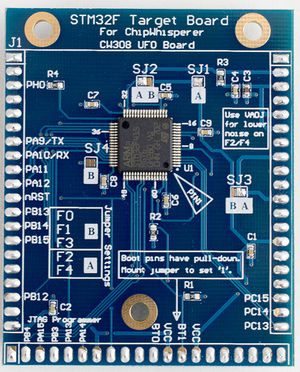
The STM32F board supports several STM32F devices in the TQFP-64 package. Various solder jumpers need to bet set to either the "A" or "B" position to select appropriate VCC supply for the different series. The following table summarizes examples of suitable devices:
| STM32F Series | Package | Device | Hardware AES | Tested | Jumper |
|---|---|---|---|---|---|
| F0 | TQFP-64 | STM32F071RBT6 | No | B* | |
| F1 | TQFP-64 | B | |||
| F2 | TQFP-64 | A | |||
| F3 | TQFP-64 | STM32F303R8T6 | Yes | No | B |
| F4 | TQFP-64 | STM32F415RGT6 | Yes | Yes | A |
* The F0 variant has a slightly different pinout, as has less VCC/GND pins and more I/O pins than other devices. The result is several I/O pins cannot be used as they are tied to VCC/GND. This will NOT affect regular usage. See details below.
VCC-Int Supply
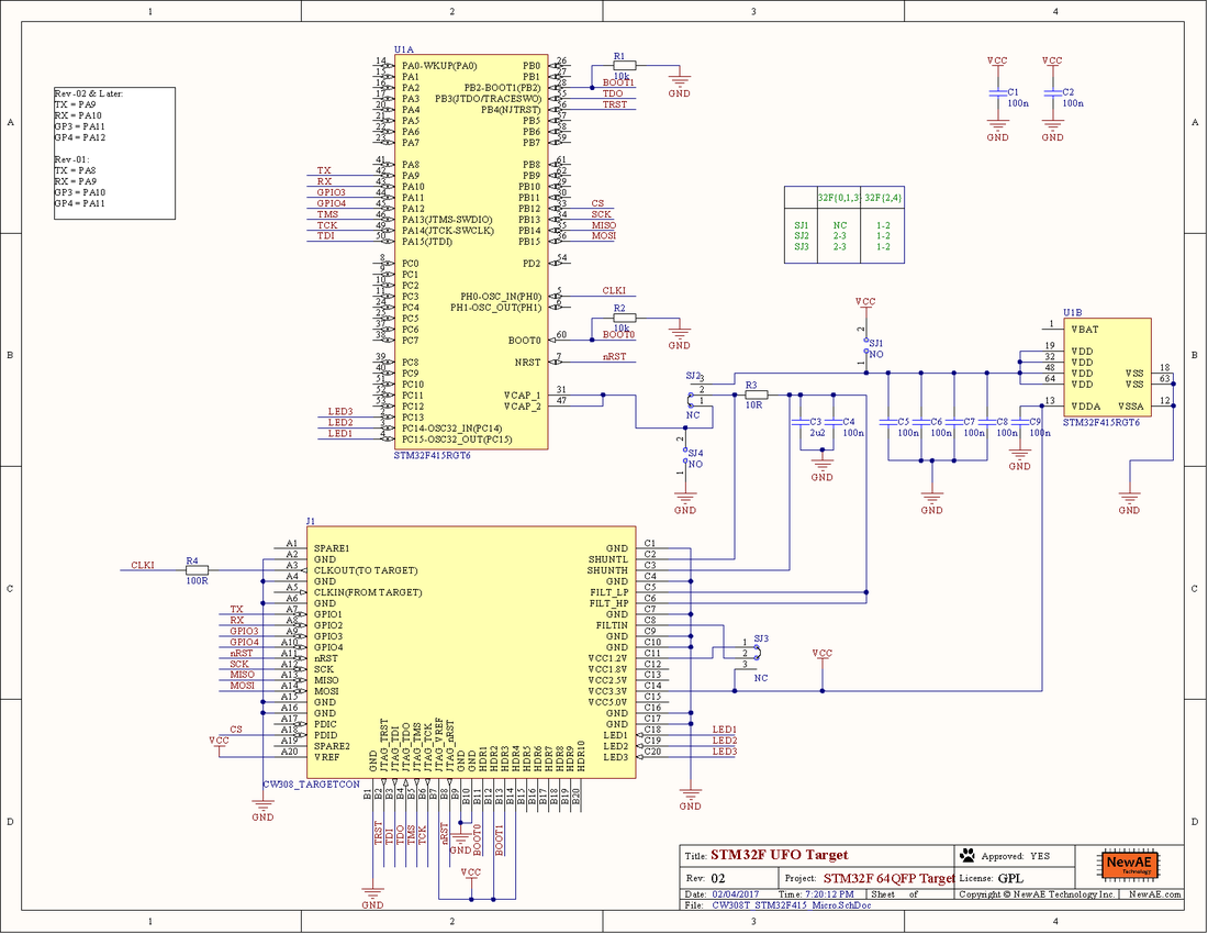
Several devices (F2, F4) have internal core voltage regulators. By default the CW308 board attempts to provide power for these pins, but the voltage may not be high enough to cause the internal regulator to disable itself. In this case you can use the VADJ regulator to ensure the internal regulator is disabled. See Targets with Internal Regulators for details.
Pin-outs across TQFP Devices
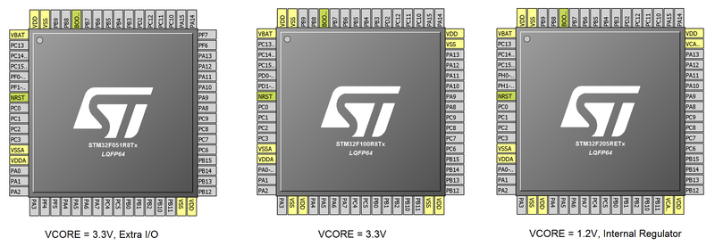
The following shows differences in pinouts between three groups of devices. The left-most is the STM32F051RB, which uses the same 3.3V VCORE as the STM32F1/F3. It has fewer VCC pins, so the I/O occupying that are VCC/GND pins on the STM32F1 (such as PF6/PF7) are tied to GND/VCC. The right-most part is the pinout of the STM32F2/F4. It has an internal regulator, where the VCAP pins are the output of this regulator (and input to the internal core logic).
Note for the devices with a 3.3V VCORE, you should not mount decoupling capacitors C5/C6/C7/C8. You will still get some leakage with those capacitors mounted, but a stronger signal is present without them.
Hardware AES
The STM32F21x, and STM32F41x/43x have hardware crypto modules (AES, DES, TDES) along with hardware hash (SHA1, MD5).
Programming Connection
The 20-pin JTAG port (J6 on CW308 Board) can be used with the ST-LINK/V2 which is a low-cost JTAG programmer.
It is also possible to use other JTAG programmers such as OpenOCD. The following command worked with an Olimex OpenOCD programmer and their OpenOCD for Windows software:
openocd
  -f path/to/board/files/cw308.cfg
  -c init
  -c targets
  -c "halt"
  -c "flash write_image erase path/to/firmware.hex"
  -c "verify_image path/to/firmware.hex"
  -c "reset run"
  -c shutdown
where the contents of cw308.cfg are
source [find interface/olimex-arm-usb-ocd-h.cfg]
source [find target/stm32f4x.cfg]
reset_config srst_only
Example Projects
WARNING: The current example projects are built for the -01 rev of the PCB. The only change is the trigger pin has changed, you will need to modify the stm32f4 HAL file to reflect the trigger is now PA12 (-02 version) instead of PA11 (-01 version).

