CW308 UFO Target
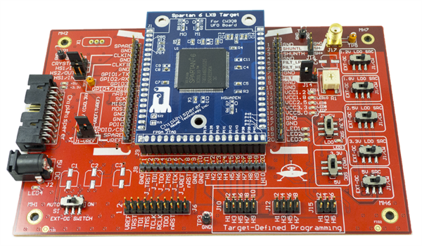
The CW308 UFO Board is a handy main-board for attacking all sorts of embedded targets. Released in 2016, it forms the basis for most of our upcoming target boards. It can be used stand-alone (with an oscilloscope) or with the ChipWhisperer-Capture hardware.
Overview
Victim Board Connectors
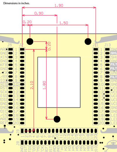
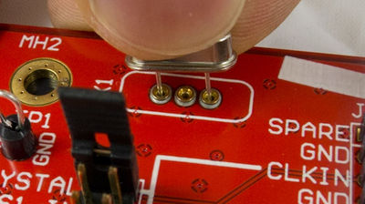
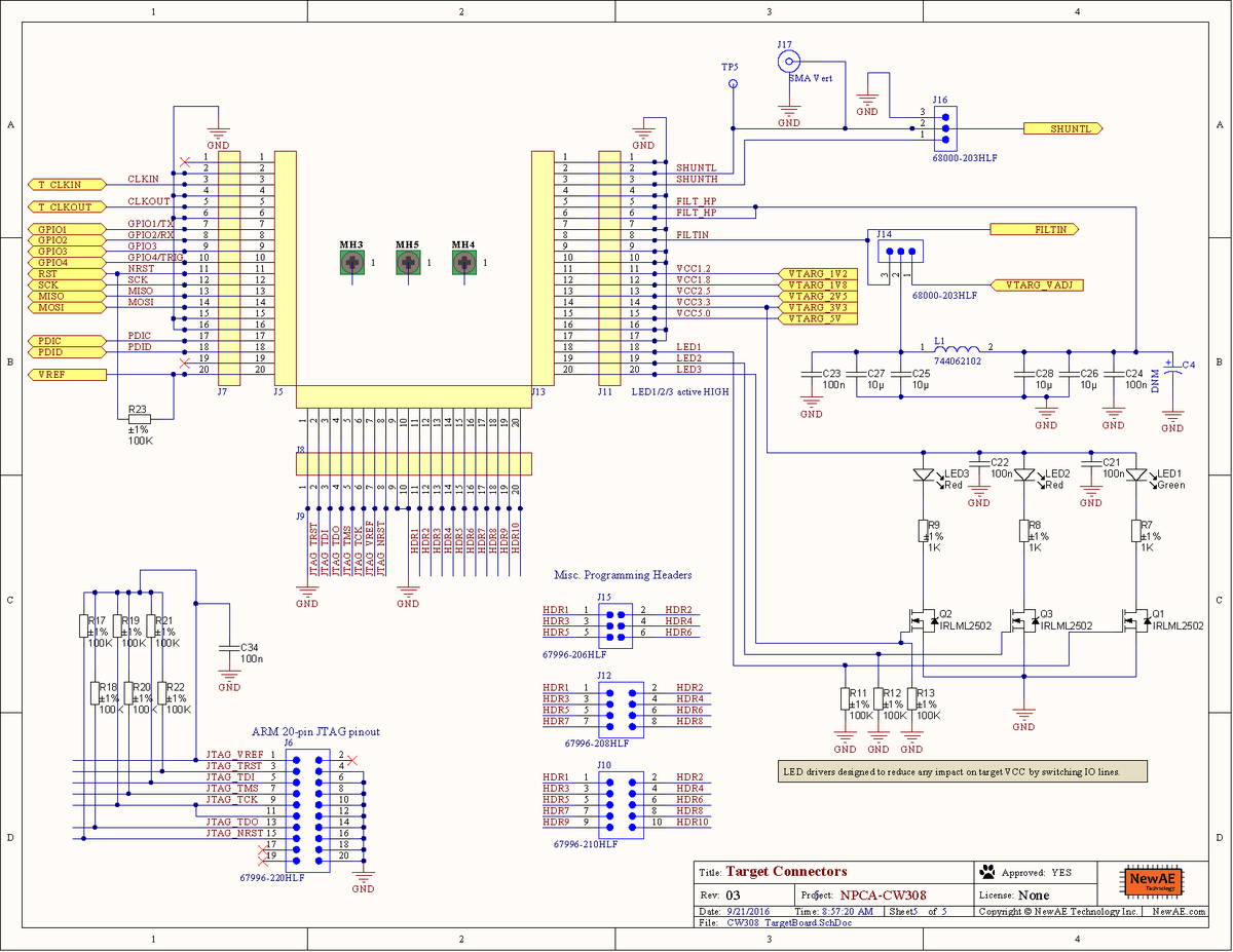
The "victim board" fits into three 20-pin female headers. They provide both electrical and mechanical connections for the board. There is optional mounting holes which can be used if additional mechanical support is required (especially if you need a locked-down victim for use with an EM probe).
The following shows the dimensions of the main connector:
| J7 (West, A) | Function | Direction | Notes |
|---|---|---|---|
| 1 | Spare | Not connected to main-board, can be used as spare I/O pin breakout. | |
| 2 | GND | ||
| 3 | CLK-IN | CW308 --> Victim | Clock to victim. |
| 4 | GND | ||
| 5 | CLKOUT | CW308 <-- Victim | |
| 6 | GND | ||
| 7 | GPIO1 | ||
| 8 | GPIO2 | ||
| 9 | GPIO3 | ||
| 10 | GPIO4 | ||
| 11 | nRST | CW308 --> Victim | 100k pull-up to VREF. |
| 12 | SCK | ||
| 13 | MISO | ||
| 14 | MOSI | ||
| 15 | GND | ||
| 16 | GND | ||
| 17 | PDIC | ||
| 18 | PDID/CS | ||
| 19 | Spare | ||
| 20 | VREF | CW308 <-- Victim | Reference voltage for I/O. MUST be set to VCC-IO voltage (3.3V, etc) or I/O lines may not work. |
| J9 (South, B) | Function | Direction | Notes |
|---|---|---|---|
| 1 | GND | ||
| 2 | JTAG_TRST | Connects to 20-pin ARM JTAG header. | |
| 3 | JTAG_TDI | Connects to 20-pin ARM JTAG header. | |
| 4 | JTAG_TDO | Connects to 20-pin ARM JTAG header. | |
| 5 | JTAG_TMS | Connects to 20-pin ARM JTAG header. | |
| 6 | JTAG_TCK | Connects to 20-pin ARM JTAG header. | |
| 7 | JTAG_VREF | Connects to 20-pin ARM JTAG header. All JTAG_ pins have 100k pull-up to this pin. Must set to appropriate value. | |
| 8 | JTAG_nRST | Connects to 20-pin ARM JTAG header. | |
| 9 | GND | ||
| 10 | GND | ||
| 11 | HDR1 | J10, J12, J15: Pin 1 | |
| 12 | HDR2 | J10, J12, J15: Pin 2 | |
| 13 | HDR3 | J10, J12, J15: Pin 3 | |
| 14 | HDR4 | J10, J12, J15: Pin 4 | |
| 15 | HDR5 | J10, J12, J15: Pin 5 | |
| 16 | HDR6 | J10, J12, J15: Pin 6 | |
| 17 | HDR7 | J10, J12: Pin 7 | |
| 18 | HDR8 | J10, J12: Pin 8 | |
| 19 | HDR9 | J10: Pin 9 | |
| 20 | HDR10 | J10: Pin 10 |
| J11 (East, C) | Function | Direction | Notes |
|---|---|---|---|
| 1 | GND | ||
| 2 | SHUNTL | Low-Side Shunt Connection (connects to SMA) | |
| 3 | SHUNTH | High-Side Shunt Connection (power input side) | |
| 4 | GND | ||
| 5 | FILT_HP | CW308 --> Victim | High-Power filter output (same as FILT_LP on this hardware) |
| 6 | FILT_LP | CW308 --> Victim | Low-Power filter output (same as FILT_HP on this hardware) |
| 7 | GND | ||
| 8 | FILTIN | CW308 <-- Victim | Input to power supply filter. |
| 9 | GND | ||
| 10 | GND | ||
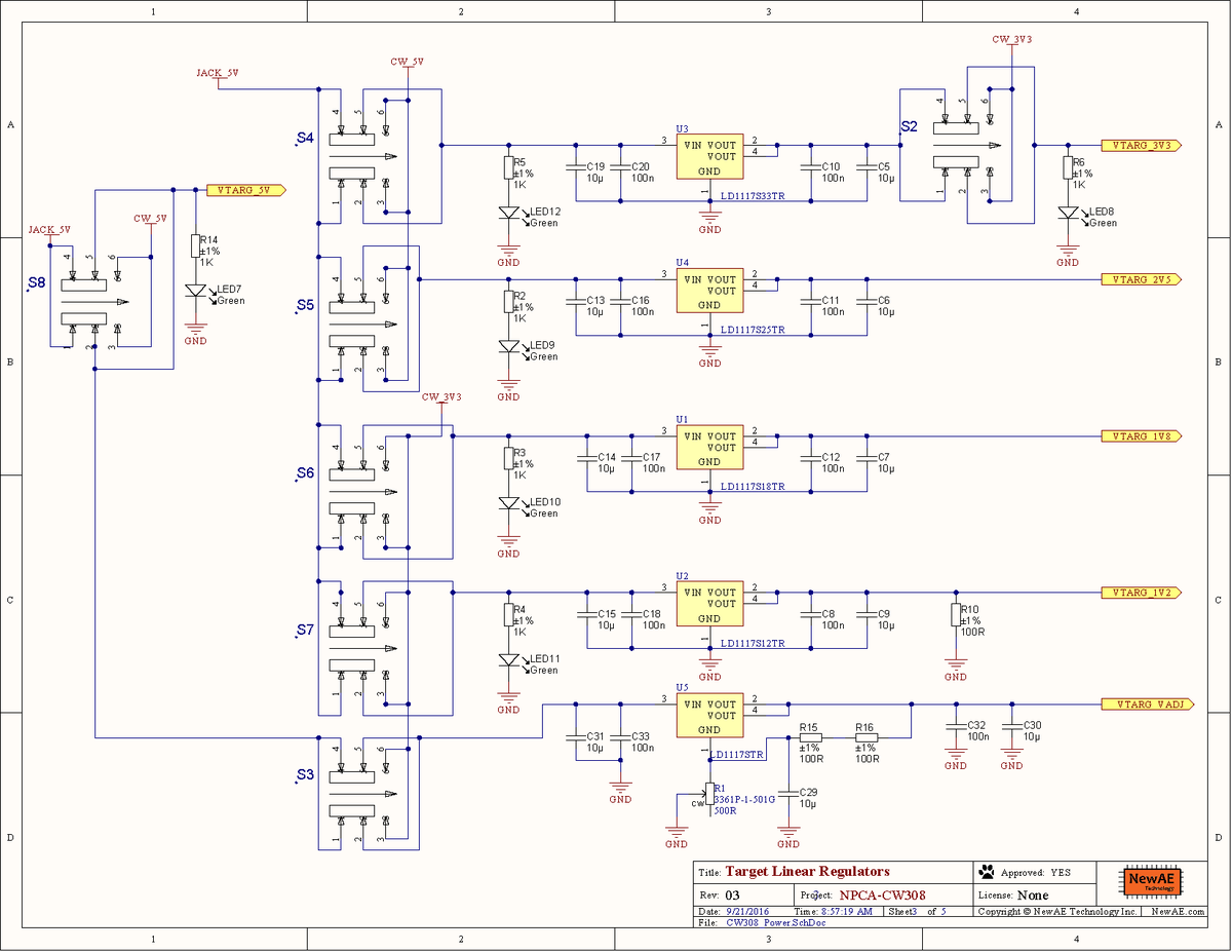
| 11 | 1.2V | CW308 --> Victim | 1.2V LDO Regulator output |
| 12 | 1.8V | CW308 --> Victim | 1.8V LDO Regulator output |
| 13 | 2.5V | CW308 --> Victim | 2.5V LDO Regulator output |
| 14 | 3.3V | CW308 --> Victim | 3.3V LDO Regulator output OR 3.3V from 20-pin connector |
| 15 | 5.0V | CW308 --> Victim | 5.0V from either DC-Power jack or 20-pin connector |
| 16 | GND | ||
| 17 | GND | ||
| 18 | LED1 | CW308 <-- Victim | Active-high buffered LED driver. 100k pull-down. |
| 19 | LED2 | CW308 <-- Victim | Active-high buffered LED driver. 100k pull-down. |
| 20 | LED3 | CW308 <-- Victim | Active-high buffered LED driver. 100k pull-down. |
Removing / Replacing Victim Boards
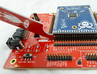
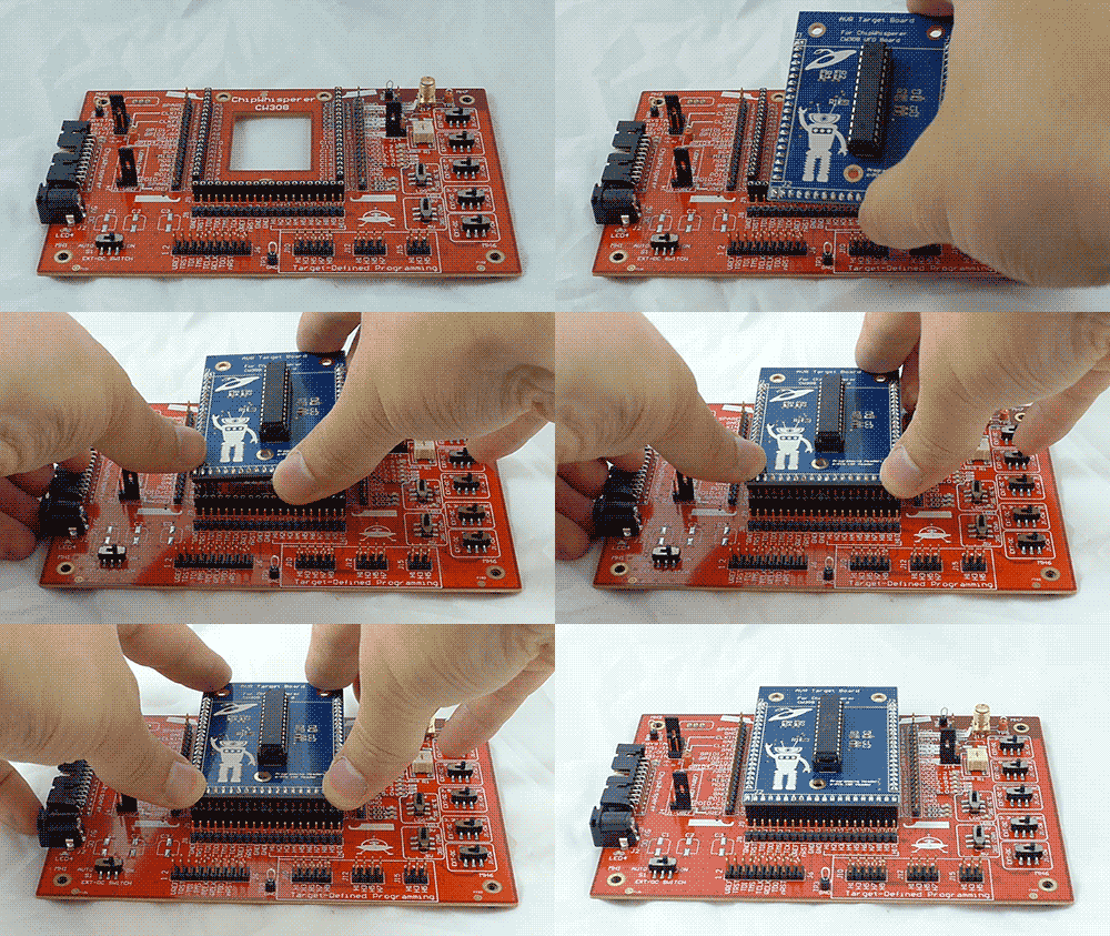
The target board is removed and replaced using the removal tool. This helps avoid bending pins:
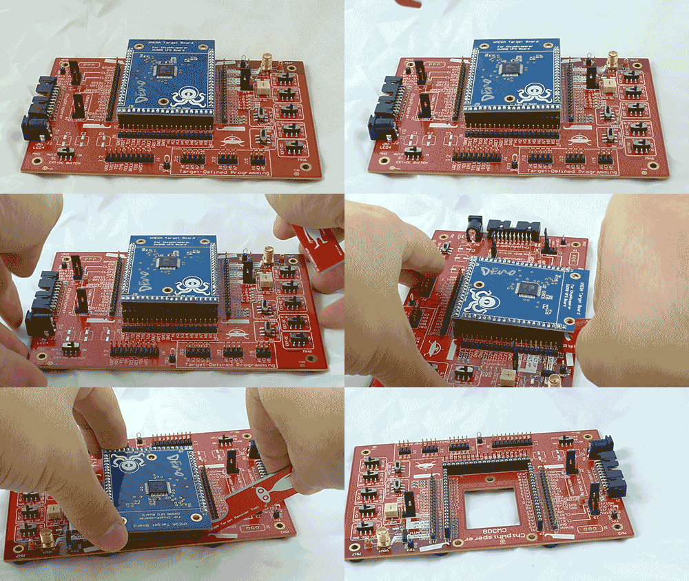
The following shows the removal process:
Adding a board involves carefully aligning the board and pushing down:
The alignment should be carefully checked if resistance is found. You may need to adjust how the board is aligned, as you should be able to press down with minimal force.
The CW308 should be turned off when swapping victim boards.
I/O Connections
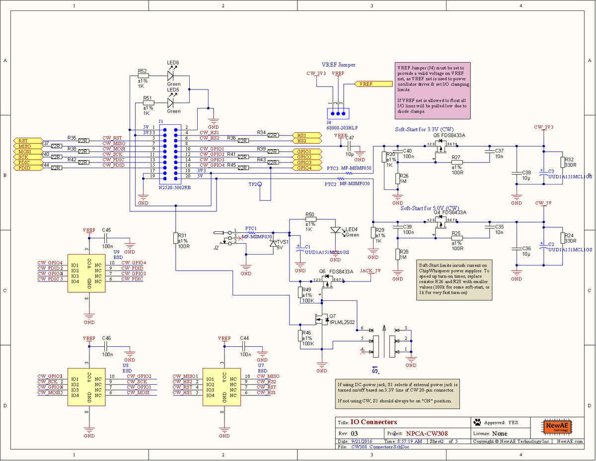
There are two main I/O connection points: the pin headers which duplicate the target board connections, and the 20-pin ChipWhisperer header.
The ChipWhisperer header pins (most of the pins on header J5) have diode protection to set a maximum voltage level. The maximum voltage is set by the voltage present on the middle pin of J4.
