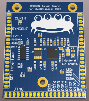
CW308T-CEC1702
| CW308T-CEC1702 | |
|---|---|
 | |
| Target Device | MCHP CEC1702 |
| Target Architecture | ARM Cortex M4F |
| Hardware Crypto | AES, SHA, RSA |
| Supported Apps | [] |
| Programmer | Generic SPI Flash Programmer |
| Status | In Development |
The CW308T-CEC1702 incorporates the main chip with a 16MB SPI flash chip and a bi-directional SPI Buffer. The target board has standard power monitoring, UART serial, and clock In/Out compatibility with the CW308. JTAG pins and many GPIO pins are also exposed for prototyping and testing use.
I/O Connections
| CW308 Pin | CEC1702 Pin | Function |
|---|---|---|
| GPIO1 | P104 (TXD0) | Serial OUTPUT from CEC1702 |
| GPIO2 | P105 (RXD0) | Serial INPUT to CEC1702 |
| GPIO3 | P030 | GPIO |
| GPIO4 | P017 | Trigger pin |
| CLKIN | XTAL2 | Optional CLKIN |
| CLKFB | P002 (PWM5) | Can output 12MHz PWM on this pin. Useful for synchronizing to internal oscillator |
| J_TRST | JTAG_RST | JTAG Reset |
| J_TDI | JTAG_TDI | JTAG TDI |
| J_TDO | JTAG_TDO | JTAG TDO |
| J_TMS | JTAG_TMS | JTAG TMS |
| J_TCK | JTAG_CLK | JTAG Clock |
| LED1 | P156 | GPIO, Breathing LED0 |
| LED2 | P157 | GPIO, Breathing LED1 |
| LED3 | PA7 | GPIO, LED |
| PDIC | SPI buffer output enable, drive high to enable SPI programming and sniffing | |
| PDID/CS | QSPI0_CS | SPI chip select for SPI flash chip |
| H1 | P040 | GPIO |
| H2 | P031 | GPIO |
| H3 | P026 | GPIO |
| H4 | P053 | GPIO |
| H5 | P054 | GPIO |
| H6 | P027 | GPIO |
| H7 | P107 | GPIO |
| H8 | P120 | GPIO |
| H9 | P112 | GPIO |
| H10 | P113 | GPIO |
Hardware Cryptography
Multi-purpose AES Cryptographic Engine
- Hardware support for ECB, CTR, CBC, and OFB AES modes
- Support for 128-bit, 192-bit and 256-bit key length
- DMA interface to SRAM, shared with Hash engine
Cryptographic Hash Engine
- Support for SHA-1, SHA-256, SHA-512
- DMA interface to SRAM, shared with AES engine
Public Key Cryptographic Engine
- Hardware support for RSA and Elliptic Curve public key algorithms
- RSA keys length from 1024 to 4096 bits
- ECC Prime Field and Binary Field keys up to 640 bits
- Microcoded support for standard public key algorithms
Other Cryptographic Features
- True Random Number Generator
- 1 Kbit FIFO
- Monotonic Counter
Programming Process
Programming the target involves writing an image into the SPI flash chip, the process is detailed below.
1) Writing and Modifying Code
The MikroC PRO for ARM IDE supports programming of the CEC1702 and comes with extensive libraries and example code. The CW308T-CEC1702 shares the same SPI configuration as all development boards currently on the market so is largely compatible with code developed on the platform. The IDE allows for editing code in both C and ASM.
2) Building a Valid SPI Image
A special image file must be generated to be compatible with the CEC1702 Boot sequence. The MikroC IDE is capable of building this image automatically but some settings must be configured before running a build.
Project > Edit Project
Select CEC1702 in the MCU Name dropbox, change the MCU Clock Frequency to 48MHz.
> General Output Settings ...
Make sure Generate BIN image file is checked. Press OK on the window and the previous edit project window.
Build > Build
The messages dialog should indicate a successful build, and the image binary can now be found in the project output folder. To confirm correct build settings, check the image binary using your SPI flash software or a HEX editor. The image binary should begin with the 8 bytes 01 00 00 3E 01 00 00 3E at offset 000000, and the rest of the program should begin at offset 000100.
3) Erasing, Loading, and Verifying the SPI Flash
The SST26VF016B flash chip can be programmed by an SPI programmer attached to the SPI pins of the CW308. Attach a jumper to J8 on the CW308, pulling nRST to GND. Ensure both the target and your SPI programmer are powered. PDIC must be driven high during the programming process to enable communication through the buffer chip.
The SST26VF016B flash chip uses global block protection that must be disabled before every write operation. This is done by sending the command code 98 to the chip before erasing or writing to the device. This can be done by configuring a custom transaction in your flash programming software. Below is a table of useful information for configuring your programming software. The Parameters listed here have been tested with the Total Phase Flash Center software and the Aardvark I2C/SPI Host adapter. See the SST26VF016B data sheet for more details.
| Parameter | Value |
|---|---|
| deviceName | SST26VF016B |
| deviceDescription | SST SST26VF016B 16 Megabyte SPI Flash |
| capacity | 16*1024*1024 |
| maxBitrate | 8*1000 |
| addressWidth | 3 |
| writeSize | 256 |
| writeTime | 64 |
| writeAutoAddressIncrementSize | 2 |
| writeAutoAddressIncrementTime | 10 |
| readDeviceIdInstruction | 0x9F |
| expectedDeviceId | \xbf\x26\x41 |
| eraseAllInstruction | 0xC7 |
| eraseAllTime | 16000 |
| userTransaction1 | \x98 |
| userTransaction1Time | 10000 |
| userTransaction1WriteEnable | false |