CW305 Artix FPGA Target
The CW305 is a FPGA target board. It brings features including a simplified USB interface for talking to the FPGA, an external PLL for adjusting frequency response, a programmable VCC-INT supply, and diode protection for use in fault injection environments. Also available with a special BGA socket, giving you the ability to perform tests on multiple FPGA devices - perfect for checking Physically Unclonable Functions (PUFs) under the exact same environmental conditions across multiple FPGAs.
This board requires an external oscilloscope or capture box for performing the power measurement. The board is designed to interface to hardware such as the ChipWhisperer-Lite 2-Part version or the CW1200 (ChipWhisperer-Pro).
Feature Overviews
USB Interface
This board uses NewAE Technology Inc's custom USB interface firmware. This firmware gives you a simple data/address bus, which you can read/write to the FPGA. The USB chip also controls FPGA configuration (which for the 7A35T device takes just under 2 seconds), the PLL, and the VCC-INT regulator. This makes it easy to script complex jobs like performing measurements at different frequencies or voltages, or reconfiguring the FPGA after a fault attempt to avoid issues with SRAM corruption.
PLL
The CDCE906 PLL means you can easily output frequencies from about 5-160 MHz (a larger range is possible but may require more care). The PLL is programmed over USB, and 3 output channels are provided (each which can be set to a different frequency). 2 route to the FPGA and 1 routes to a SMA connector. This allows you to synchronize external devices or boards to the oscillator driving your FPGA design.
Power Supply
Three switching regulators are provided - two fixed for VCC-AUX and VCC-IO, along with a VCC-INT supply which can be programmed over the range of 0.8V-1.10V (this is a software limit to prevent you from damaging the FPGA, this can be overridden if you need to provide about a 0.65-1.5V range). Optional linear regulators can plug into the VCC-AUX and VCC-IO supplies which provide lower-noise operation (but with a reduced current limit compared to the switching supplies).
External banana connectors make is simply to power the VCC-INT from a low-noise bench supply. This can improve side-channel analysis measurements by reducing noise in the shunt measurement compared to the on-board switching supply.
An on-board DMM measures the VCC-INT supply and provides easy visual feedback so you can confirm settings without needing to attach a meter.
Shunt Measurement
A resistive shunt is provided in the VCC-INT supply, with an optional shunt in the VCC-AUX line. The resistive shunt can be measured using a differential probe on 0.1" spacing, using the SMAs, or using the on-board 20dB LNA. The LNA makes it easier to measure with standard oscilloscopes that don't measure the very small variations you find in power analysis.
Fault Injection
This board is designed to facilitate all forms of fault injection. Resitive and diode protection prevents transients on the VCC-IO of the FPGA from affecting the USB interface chip. The USB chip itself provides high-speed FPGA reconfiguration to simplify repetitive fault attacks where you need to reconfigure the FPGA. The USB interface can also monitor the INITB pin of the FPGA, which can be used with the continous CRC verification feature to determine when reconfiguration is required.
The PCB features mounting holes and alignment features for use with an X-Y table (suitable for both EM fault injection and H-Field probes).
The VCC-INT supply can be disconnected from the filtering capacitors to allow using the SMA jacks as a method of inserting voltage faults without fighting the output capacitance of the power supply.
The ChipWhisperer Crowbar fault injection can also be used with this board, which requires either the ChipWhisperer-Lite 2-Part version (CW1173-2PART) or CW1200.
Hardware Details
VCC-INT Routing
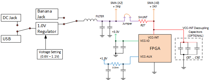
The following shows details of how the power supplies are routed on the CW305 board:
Details of each section are shown here:
DC Jack / USB Power
There are two main sources of power which can be used for all FPGA power supplies (VCC-INT, VCC-IO, and VCC-AUX). By default this is the USB connector, but this is limited by USB specs to a maximum of 500 mA.
If using a larger design in the FPGA you may exceed these limits, in which case you must move the switch to use the DC-Jack. This jack requires a 5.0V power supply capable of a suitable amount of current for your design (suggested: 2.0A).
Internal / External VCC-INT
The internal power supply provides a source of 1.0V for the VCC-INT. This supply can be programmed slightly above/below 1.0V to compare the effects of different VCC-INT supplies on the FPGA design. Details of the power supply are given in section TODO XREF. The internal supply can provide up to 6.0A for the VCC-INT rail.
There is also two banana jacks which can be connected to a 1.0V lab supply. You must be very careful to ensure you do not exceed 1.10V on this input, as beyond that range you risk damaging the FPGA.
The choice of internal/external is selected with the switch. There is a ferrite bead + large capacitors after this switch, so note that you cannot use the banana jack inputs as a voltage glitch insertion method. Instead you must insert them directly into the SMA connectors
Shunt Resistor Connections
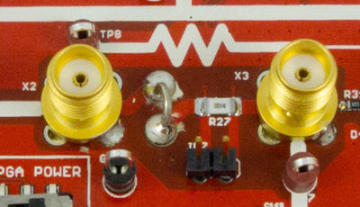
The following shows the components around the shunt resistor:
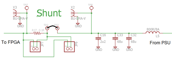
Schematically, this is shown below. NOTE: the schematic flows in the "opposite" direction of the PCB. In the PCB power flows left to right, in the schematic it flows right to left.
A brief description of each element is given below.
SMA Connectors / Test Points
The SMA connectors provide access to both sides of the shunt. The "high side" comes from the power supply with substantial filter capacitors, and the "low side" goes directly to the FPGA VCC-INT network. The VCC-INT network may or may not have decoupling capacitors mounted (this is an ordering option).
In addition, two test points are provided on each side that are suitable for use with an oscilloscope probe. It is strongly recommended to use a SMA to BNC cable (such as Cinch Connectivity P/N 415-0028-024 available from Digikey) to view the power measurement instead of these test points, as the SNR of the oscilloscope probe will typically be considerably worse than via the SMA connector.
The SMA connector can also be used when inserting faults into the FPGA. If using the ChipWhisperer crowbar fault generator, simply connect the crowbar output to connector X3. If using an external fault amplifier, you will also connect to X3 but will also need to remove the jumper (described below).
Jumper
In some circumstances you may wish to entirely remove the shunt resistor. This is typically the case when performing fault insertion, where the large "filter" capacitors present on the high side of the shunt resistor will drastically reduce the slew rate of your fault amplifier.
Alternatively, you may wish to use a current transformer or similar current probe which requires a method of inserting a sensor into the VCC-INT path.
For these uses test point TP2 and TP3 have gold-plated "nails" soldered into them, and a wire bridge soldered between the test points. This wire bridge can be removed by either cutting (with wire cutters) or desoldering. The gold-plated nails provide a mechanically strong base which allows you to perform this operation without risking damage to the CW305 PCB.
If using a current probe, you can either (1) solder a wire between TP2 and TP3, or (2) use two SMA connectors to route the power between X2 and X3. Clamp your current probe onto the bare wire used to route the signal between these (you'll need a custom cable without the shield most likely).
The gold-plated nails that require soldering are used instead of a switch or jumper to reduce the resistance in the measurement path. Typical switches provide too high of a contact resistance for the potential current draw of a large design in the FPGA, which would reduce the SNR at the measurement point.
Shunt Resistor
The shunt resistor is a 1206 size resistor mounted at position R27. The value of this resistor will vary between the various variants of the assembled board.
Two 0.100" (2.54mm) headers are provided for measurement with a differential probe. One (JP7) is directly across the resistor, and the other (JP6) is on the top right side of the PCB. JP6 is designed to be used with a NewAE Technology Inc. differential probe (which requires a separate power supply for this differential probe).
VCC-INT Decoupling Capacitors
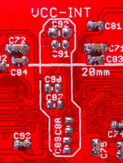
The optional decoupling capacitors for the VCC-INT rail are shown on the underside of the PCB here:
This capacitors are typically not mounted when using the shunt resistor to measure power waveforms.
VCC-AUX Shunt Resistor
The VCC-INT shunt is the primarily power measurement point, as it provides power measurement for both designs inside the FPGA, along with the logic responsible for decrypting bitstreams (as reported at https://eprint.iacr.org/2016/249.pdf).
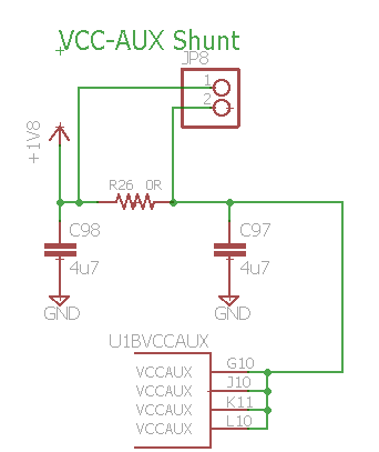
There may be additional information in the VCC-AUX power supply however, for example monitoring JTAG state transitions. There is a secondary shunt position (by default with no shunt mounted) for exploration of the VCC-AUX power supply. This can be seen in the schematic here:
The shunt is located on the rear side of the PCB, as shown here:
If using this shunt, you must remove resistor R26 (which has a metal slug 0-ohm resistor mounted) and replace with an appropriately sized 0805 resistor (suggested: 1 ohm). You must also remove capacitor C98, C95, C97, C94, and C93. They can be seen in the above photo.
Shunt Selection
Fault Injection
FPGA Configuration
Software Details
The ChipWhisperer software is used to communicate with this board. This can be used either as part of the GUI (i.e., using the CW305 within the ChipWhisperer-Capture), or by importing Python modules and communicating with the CW305.
Driver and Software Installation
Programmatic Usage
Using from Other Languages
The provided modules are written in Python, but any language which is supported by libusb can talk to the hardware. This will require you to write your own lower-layer driver and is officially unsupported by NewAE.
If using from other software (such as MATLAB), it is suggested to call the command-line interface (described below) or otherwise use the existing Python interface. The Python interface is guaranteed to maintain compatibility with future changes in the SAM3U firmware.
