| As of August 2020 the site you are on (wiki.newae.com) is deprecated, and content is now at rtfm.newae.com. |
CW308T-CEC1702
| CW308T-CEC1702 | |
|---|---|
 | |
| Target Device | MCHP CEC1702 |
| Target Architecture | ARM Cortex M4F |
| Hardware Crypto | AES, SHA, RSA |
| Supported Apps | SimpleSerial AES, others possible |
| Programmer | Generic SPI Flash Programmer |
| Status | In Development |
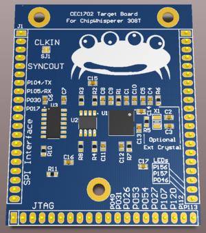
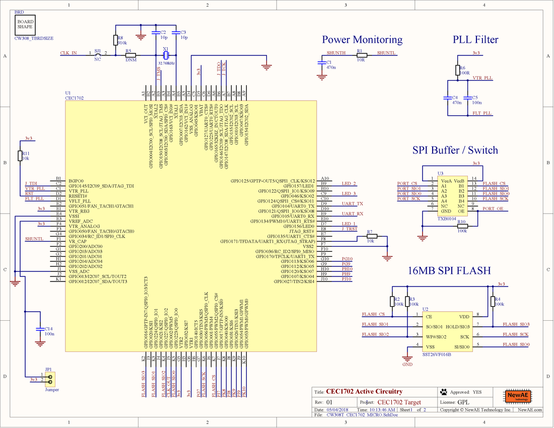
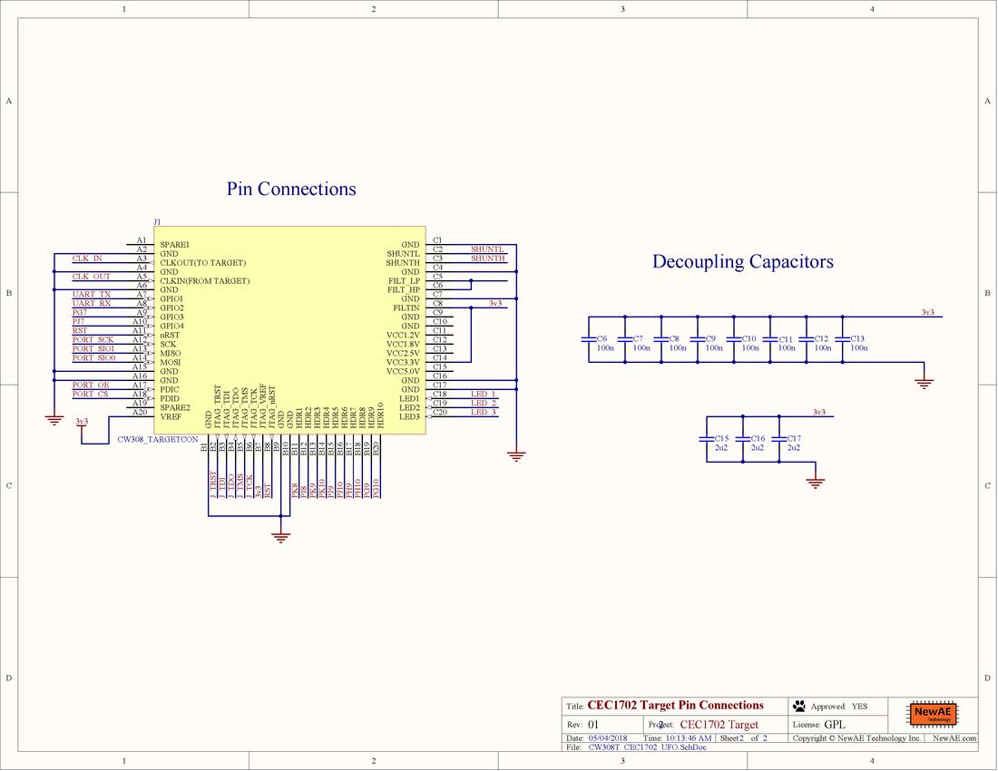
The CW308T-CEC1702 incorporates the main chip with a 16MB SPI flash chip and a bi-directional SPI Buffer. The target board has standard power monitoring, UART serial, and clock In/Out compatibility with the CW308. JTAG pins and many GPIO pins are also exposed for prototyping and testing use.
This device is interesting in that it has a lot of hardware crypto and security functionality.
Contents
I/O Connections
| CW308 Pin | CEC1702 Pin | Function |
|---|---|---|
| GPIO1 | P104 (TXD0) | Serial OUTPUT from CEC1702 |
| GPIO2 | P105 (RXD0) | Serial INPUT to CEC1702 |
| GPIO3 | P030 | GPIO |
| GPIO4 | P017 | Trigger pin |
| CLKIN | XTAL2 | Optional CLKIN |
| CLKFB | P002 (PWM5) | Can output 12MHz PWM on this pin. Useful for synchronizing to internal oscillator |
| J_TRST | JTAG_RST | JTAG Reset |
| J_TDI | JTAG_TDI | JTAG TDI |
| J_TDO | JTAG_TDO | JTAG TDO |
| J_TMS | JTAG_TMS | JTAG TMS |
| J_TCK | JTAG_CLK | JTAG Clock |
| LED1 | P156 | GPIO, Breathing LED0 |
| LED2 | P157 | GPIO, Breathing LED1 |
| LED3 | PA7 | GPIO, LED |
| PDIC | SPI buffer output enable, drive high to enable SPI programming and sniffing | |
| PDID/CS | QSPI0_CS | SPI chip select for SPI flash chip |
| H1 | P040 | GPIO |
| H2 | P031 | GPIO |
| H3 | P026 | GPIO |
| H4 | P053 | GPIO |
| H5 | P054 | GPIO |
| H6 | P027 | GPIO |
| H7 | P107 | GPIO |
| H8 | P120 | GPIO |
| H9 | P112 | GPIO |
| H10 | P113 | GPIO |
Hardware Cryptography
Multi-purpose AES Cryptographic Engine
- Hardware support for ECB, CTR, CBC, and OFB AES modes
- Support for 128-bit, 192-bit and 256-bit key length
- DMA interface to SRAM, shared with Hash engine
Cryptographic Hash Engine
- Support for SHA-1, SHA-256, SHA-512
- DMA interface to SRAM, shared with AES engine
Public Key Cryptographic Engine
- Hardware support for RSA and Elliptic Curve public key algorithms
- RSA keys length from 1024 to 4096 bits
- ECC Prime Field and Binary Field keys up to 640 bits
- Microcoded support for standard public key algorithms
Other Cryptographic Features
- True Random Number Generator
- 1 Kbit FIFO
- Monotonic Counter
Firmware
The firmware provided with Chipwhisperer (or its own repo) is designed to work with the MikroC PRO for ARM IDE. This IDE supports the many peripherals of the CEC1702, including the hardware security features and comes with extensive libraries and example code. The board layout has been designed to be compatible with many of the provided examples, while some others can be easily modified to work with the CW308T-CEC1702. After the binaries have been created, they can either be loaded into SPI Flash or directly into RAM via JTAG.
Creating and Modifying Examples
The following notes may prove useful when using mikroC PRO examples or creating your own:
- Any example which uses UART1 needs to be changed to use UART0 by changing the UART1_* functions to UART0_*.
- The plain text and encrypted text buffers need to be 16 byte aligned for the CEC1702's DMA to function properly. If the aes_crypt() call fails or the encryption never completes, this may be the cause. See simpleserial_base.c or mikroC PRO's AES examples for examples of this.
- All variable declarations need to be done at the beginning of functions, before any variables are modified or functions are called.
- The mikroC PRO compiler may have strange sizes for integer constants, meaning changing 4 8 bit numbers into a 32 bit number via bitshifts may not work as intended. Instead, using memcpy() may prove easier and more reliable.
- When using mikroC PRO's "Clean Project Folder", ensure that .mcpar, .c, .h, and .xml files are not selected, as this will cause the source/project/Flash Center
- The port base for use with the GPIO library is actually GPIO_PORT_xxx_xxx, not _GPIO_PORT_xxx_xxx. Additionally, this is not a pointer, meaning the address of this variable needs to be passed to the gpio functions
- There are no GPIO library functions to write or read from pins. Instead, use GPIO_OUTPUT_xxx_xxx.Bn/GPIO_INPUT_xxx_xxx.Bn for bit n of pin range xxx-xxx.
Compilation Settings
Project > Edit Project
Select CEC1702 in the MCU Name dropbox, change the MCU Clock Frequency to 48MHz.
If you want to program and run off of the SPI flash, additional configuration is needed:
> General Output Settings ...
Make sure Generate BIN image file is checked. Press OK on the window and the previous edit project window.
Build > Build
The messages dialog should indicate a successful build, and the image binary (PROJECTNAME_img.bin) and hex (PROJECTNAME.hex) can now be found in the project output folder. To confirm correct build settings, check the image binary using your SPI flash software or a HEX editor. The image binary should begin with the 8 bytes 01 00 00 3E 01 00 00 3E at offset 000000, and the rest of the program should begin at offset 000100.
Programming the Device
The CEC1702 supports loading code in two ways: from external flash memory into RAM and directly into RAM over JTAG.
Programming the SPI Flash
The SST26VF016B flash chip on the target board can be programmed by an SPI programmer attached to the SPI pins of the CW308. To program the chip, the nRST chip must be pulled to ground by holding the nRST button down or by connecting a jumper to J8 on the CW308. Additionally, the SDIC pin must be driven high during the programming process the enable communication through a buffer chip.
The SST26VF016B flash chip uses global block protection that must be disabled before every write operation. This is done by sending the command code 98 to the chip before erasing or writing to the device. This can be done by configuring a custom transaction in your flash programming software. Below is a table of useful information for configuring your programming software. The Parameters listed here have been tested with the Total Phase Flash Center software and the Aardvark I2C/SPI Host adapter. Additionally, a Total Phase Flash Center script is provided with the firmware for additional reference. See the SST26VF016B data sheet and the manual for your SPI flash program for more details.
| Parameter | Value |
|---|---|
| deviceName | SST26VF016B |
| deviceDescription | SST SST26VF016B 16 Megabyte SPI Flash |
| capacity | 16*1024*1024 |
| maxBitrate | 8*1000 |
| addressWidth | 3 |
| eraseInstruction | 0x20 |
| eraseSize | 4*1024 |
| eraseTime | 18000 |
| writeSize | 256 |
| writeTime | 64 |
| writeAutoAddressIncrementSize | 2 |
| writeAutoAddressIncrementTime | 10 |
| readDeviceIdInstruction | 0x9F |
| expectedDeviceId | \xbf\x26\x41 |
| readInstruction | 0x03 |
| eraseAllInstruction | 0xC7 |
| eraseAllTime | 16000 |
| userTransaction1 | \x98 |
| userTransaction1Time | 10000 |
| userTransaction1WriteEnable | false |
Programming over JTAG/SWD
In addition to the SPI flash method, the CEC1702 can be temporarily (until power off) programmed using a JTAG debugger. This has been tested using Ozone V2.56d with a j-Trace Pro from Segger. The mikroC PRO IDE also supports programming and debugging using the Segger.
Note that the CEC1702 only supports JTAG when the Debug Select bit (Byte 482 Bit[6]) of EFUSE is 0 and SWD when the Debug Select bit is 1. If one does not work, try the other.
Load the image binary on to the flash chip and verify that the write was performed. If verification fails, ensure the nRST pin was held low for the entirety of the erase/write/verify cycle. If verification still fails, refer to the data sheet and your programming software manual to make sure the necessary command codes were sent in the appropriate order.
Running the Program
If you programmed the device via SPI flash, remove the nRST jumper/release the nRST button and disconnect the 3.3V source from PDIC. If you loaded your code from JTAG, hit go on your debugging software.
Performing CPA Attacks
The CEC1702 has no option to run off on an external clock. To make CPA attacks easier, a 12MHz PWM signal is generated on the CLKOUT pin. This can be used by putting a jumper on the lower HS1/IN pins on J3 and running the ChipWhisperer off of the ExtClk.
ATE and EFUSE
The CEC1702 ships in ATE mode suppliers, which prevents booting off of SPI flash and seems to mess with the UART baud rate (57600 baud corresponded to 32000 baud). Note the CW308T-CEC1702 target boards have this disabled as part of the production process / test procedure.
The device can be changed into normal mode by setting Byte 35 Bit[7] of the EFUSE memory. This can be done via an external SPI flash such as the mikroProg, or by loading a program that modifies the bits via JTAG. For additional information, see the CEC1702 datasheet and errata. Before modifying the EFUSE, keep the following in mind:
- EFUSE bits are one time programmable (OTP) to 1. This means there's no way to set the bits back to 0 once they are set to 1.
- To modify the EFUSE, VREF must be set to between 1.52V and 1.6V.
- Make sure that FSOURCE_EN_READ and FSOURCE_EN_PRGM are never set to 1 at the same time, as this will short ground and power.
- Note that both the EFUSE instructions in the CEC1702 datasheet and mikroC PRO's EFUSE program rely on VREF being set to ground while FSOURCE_EN_READ and FSOURCE_EN_PRGM are being switched. Instead, to modify the EFUSE, set both to 0, wait for the registers to be set, then set the appropriate bit.
- Some additional features of the EFUSE include setting keys for flash decryption and authentication by the bootloader.
You can see an example program that works with the CW308T-CEC1702 device at [1](https://github.com/newaetech/chipwhisperer-target-cec1702).
To use E-FUSE with the CW308T, you will need to use a jumper wire. To do this:
- Using a screwdriver, adjust VADJ trimmer to output 1.60V. Note you might need to switch the V-ADJ source voltage.
- Jumper the VADJ output to the VFUSE header pin.

