| As of August 2020 the site you are on (wiki.newae.com) is deprecated, and content is now at rtfm.newae.com. |
Difference between revisions of "Tutorial CW305-3 Clock Glitching"
(→Background) |
(→Glitch Setup) |
||
| Line 9: | Line 9: | ||
= Glitch Setup = | = Glitch Setup = | ||
| − | == Hardware Setup == | + | == Hardware/Software Setup == |
| − | + | The hardware setup for this tutorial is largely the same as [[Tutorial CW305-1 Building a Project]]. Start the hardware setup by following those steps (connect the boards, run the example script, and upload the bitstream). Then, we need to make a few changes to our setup. | |
| − | + | ||
| − | + | In the previous examples, we wanted to clock our Artix-7 from the target board's PLL. Now, we want to inject glitches into this clock, so we want to use the clock generated by our capture hardware. To do this, we need to change switch '''J16''' to '''1'''. This switch will force the FPGA to use the ChipWhisperer's input clock instead of the PLL. | |
| − | - ChipWhisperer clock output | + | |
| + | Next, we need to generate our own clock signal. Set up the ChipWhisperer's CLKGEN output to run at 10 MHz, and use CLKGEN x4 as the ADC clock source: | ||
| + | |||
| + | [[File:CW305Clkgen.PNG]] | ||
| + | |||
| + | Then, set up the glitch module to use CLKGEN as the input clock and set the glitch trigger to external single-shot. We'll be playing with the rest of the settings later. | ||
| + | |||
| + | [[File:CW305GlitchModule.PNG]] | ||
| + | |||
| + | Finally, under CW Extra Settings, change the Target HS IO-Out to use the Glitch Module output. Capture a trace and make sure you can see a glitch in the power. For example, here is a trace with a visible glitch from samples 30 to 35. (You might need to change the glitch width and offset - this screenshot was captured using 30% and 10%.) | ||
| + | |||
| + | [[File:CW305GlitchExample.PNG]] | ||
== Glitch Explorer == | == Glitch Explorer == | ||
| − | + | Once we've gotten clock glitches working, the objective is to find a set of glitch parameters that cause the encryption process to fail. We can do this automatically using the glitch explorer, so let's set this up to search for glitches. | |
| − | + | ||
| − | + | The first thing we need to do is get our FPGA to use a fixed plaintext and key. If we change the inputs on every capture, it'll be more difficult to tell when a glitch was successful. The rest of this tutorial will use the fixed key <code>2B 7E 15 16 28 AE D2 A6 AB F7 15 88 09 CF 4F 3C</code> and the fixed plaintext <code>5C 69 2F 91 03 B2 30 29 14 D7 E5 55 E4 DC EE 49</code>, but you can use any key and plaintext. | |
| − | + | ||
| + | Using our fixed key and plaintext, we can set up the glitch explorer to detect when we've successfully glitched the FPGA. Open the glitch explorer, then click Capture 1 to see the format of the output. With the plaintext and key mentioned above, the received output is <code>'06f36a65e8a99ff8907b2e5e5ddd77de'</code>. Set the glitch explorer's normal/successful responses to check for this string. Then, set up two tuning parameters to sweep the glitch module's width and offset. When everything is set up, your glitch explorer should look like: | ||
| + | |||
| + | [[File:CW305GlitchExplorer.PNG]] | ||
| + | |||
| + | Once everything is ready, click <code>Use this value</code> and start capturing. | ||
= Results = | = Results = | ||
Revision as of 07:39, 18 January 2017
The goal of this tutorial is to apply clock glitching to the CW305 Artix target, causing it to produce erroneous results during the encryption process. This isn't the most interesting software to glitch - in Tutorial A2 Introduction to Glitch Attacks (including Glitch Explorer), we glitched past a password check, which is a much more rewarding target. However, the setup and process in this tutorial is applicable to a wide range of FPGA programs.
Contents
Background
In the previous tutorials, we said that our FPGA implementation of AES executes each round of the algorithm in a single clock cycle. This probably means that there's one 128-bit port used to store the internal state. On each clock cycle, this state is fed through a couple of different blocks (SubBytes(), ShiftRows(), MixColumns(), and AddRoundKey()), and the output is stored back into the state port.
Our goal in this tutorial is to cause the AES execution to fail by applying clock glitches. If we trigger a short clock glitch right next to a clock edge, we might be able to corrupt some of the bits of the state array. If we can manage this, the output ciphertext will be totally different! Remember that one of the primary goals of cryptographic algorithms is diffusion: if we change a single bit of the input, the round function will cause that one bit to affect all 128 bits of the output.
In this tutorial, we'll say that a successful glitch is any glitch that causes the ciphertext to change. However, at the end of the tutorial, we'll look a bit deeper into the exact position and magnitude of these glitches to see exactly how our glitches are changing the output.
Glitch Setup
Hardware/Software Setup
The hardware setup for this tutorial is largely the same as Tutorial CW305-1 Building a Project. Start the hardware setup by following those steps (connect the boards, run the example script, and upload the bitstream). Then, we need to make a few changes to our setup.
In the previous examples, we wanted to clock our Artix-7 from the target board's PLL. Now, we want to inject glitches into this clock, so we want to use the clock generated by our capture hardware. To do this, we need to change switch J16 to 1. This switch will force the FPGA to use the ChipWhisperer's input clock instead of the PLL.
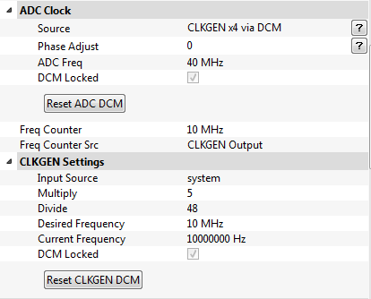
Next, we need to generate our own clock signal. Set up the ChipWhisperer's CLKGEN output to run at 10 MHz, and use CLKGEN x4 as the ADC clock source:
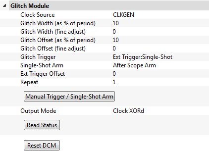
Then, set up the glitch module to use CLKGEN as the input clock and set the glitch trigger to external single-shot. We'll be playing with the rest of the settings later.
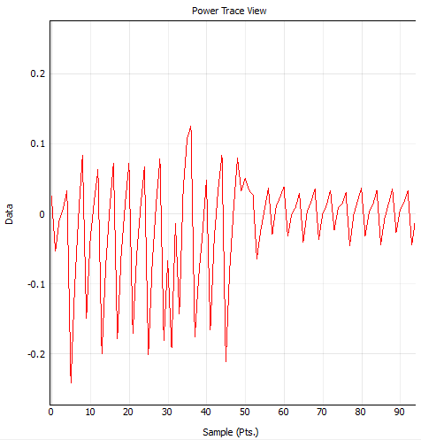
Finally, under CW Extra Settings, change the Target HS IO-Out to use the Glitch Module output. Capture a trace and make sure you can see a glitch in the power. For example, here is a trace with a visible glitch from samples 30 to 35. (You might need to change the glitch width and offset - this screenshot was captured using 30% and 10%.)
Glitch Explorer
Once we've gotten clock glitches working, the objective is to find a set of glitch parameters that cause the encryption process to fail. We can do this automatically using the glitch explorer, so let's set this up to search for glitches.
The first thing we need to do is get our FPGA to use a fixed plaintext and key. If we change the inputs on every capture, it'll be more difficult to tell when a glitch was successful. The rest of this tutorial will use the fixed key 2B 7E 15 16 28 AE D2 A6 AB F7 15 88 09 CF 4F 3C and the fixed plaintext 5C 69 2F 91 03 B2 30 29 14 D7 E5 55 E4 DC EE 49, but you can use any key and plaintext.
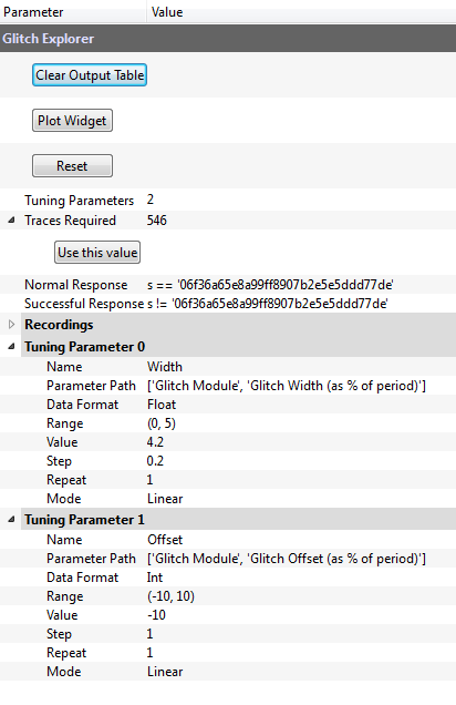
Using our fixed key and plaintext, we can set up the glitch explorer to detect when we've successfully glitched the FPGA. Open the glitch explorer, then click Capture 1 to see the format of the output. With the plaintext and key mentioned above, the received output is '06f36a65e8a99ff8907b2e5e5ddd77de'. Set the glitch explorer's normal/successful responses to check for this string. Then, set up two tuning parameters to sweep the glitch module's width and offset. When everything is set up, your glitch explorer should look like:
Once everything is ready, click Use this value and start capturing.
Results
- Glitch explorer plot - Examples of erroneous output - Repeatability
Further Analysis
- AES intermediate script - Outline code process - Show code in appendix - Show output plots


