| As of August 2020 the site you are on (wiki.newae.com) is deprecated, and content is now at rtfm.newae.com. |
Difference between revisions of "Tutorial CW305-4 Voltage Glitching with Crowbars"
(→Hints) |
(→Hardware Setup) |
||
| Line 14: | Line 14: | ||
= Setup = | = Setup = | ||
== Hardware Setup == | == Hardware Setup == | ||
| − | To set up the hardware for voltage glitching, only one extra connection is required. Connect an SMA cable between the ChipWhisperer's glitch output and the CW305 connector labeled X3: | + | To set up the hardware for voltage glitching, only one extra connection is required compared to the setup for power analysis. Connect an SMA cable between the ChipWhisperer's glitch output and the CW305 connector labeled X3: |
| − | [[File: | + | [[File:CW305_CWLite_VCCGlitch.jpg|800px]] |
Note that the original SMA cable (connected to the ChipWhisperer's Measure input) is not required for voltage glitching - if you only have one cable, you can just move it over. However, it is helpful to have power traces to see what effects the voltage glitches are having on the power rails, so connect both if you can. | Note that the original SMA cable (connected to the ChipWhisperer's Measure input) is not required for voltage glitching - if you only have one cable, you can just move it over. However, it is helpful to have power traces to see what effects the voltage glitches are having on the power rails, so connect both if you can. | ||
Revision as of 13:23, 19 January 2017
Our final goal with the CW305 Artix target is to experiment with voltage glitching. This is the CW305 equivalent of the VCC glitch attack done in Tutorial A3 VCC Glitch Attacks.
Background Information
The ChipWhisperer capture hardware comes with a glitch output, which is connected to a power MOSFET in the following configuration:
(image)
This circuit allows us to temporarily ground the Artix power rails. If these short-circuit events are timed very precisely, they can cause all kinds of fun effects in the FPGA's operation.
Voltage glitching works quite well against microcontrollers: it's pretty straightforward to use these glitches to target a specific point in an algorithm's execution. However, voltage glitching is not as easy on an FPGA target. FPGAs can perform many operations in parallel: they are not limited to one instruction of arithmetic per clock cycle. This parallel execution makes it very tricky to focus on a specific operation. There are also some serious practical concerns:
- The Artix-7 uses SRAM to store its configuration files (ie: the contents of the bitstream). SRAM is a form of volatile memory, which means that it only stores data until the device is turned off. If we cut off the power to our FPGA for too long, it's possible for some of this configuration data to be lost. We've found that around 1000 bits can be corrupted with a 600 ns glitch, but this will be device- and environment-dependent. If you find that your device isn't working properly, your first thought should be to reprogram the bitstream.
- If we ground the FPGA's power pins, then the power supply will effectively be driving the shunt resistor. With a supply voltage of 1.0 V and a 0.5 ohm shunt, this is a 2 A current; with a 0.1 ohm shunt, this is 10 A. It's probably a good idea to use an external power supply for this type of glitch.
Setup
Hardware Setup
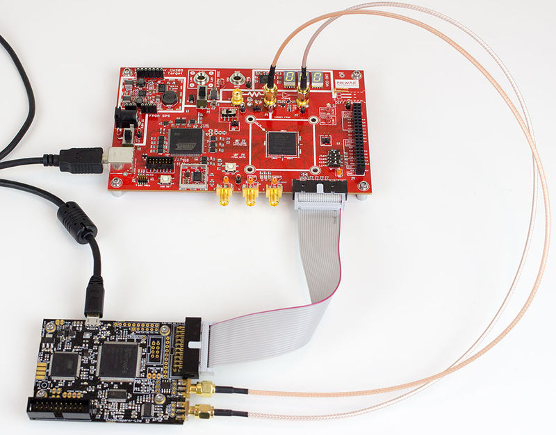
To set up the hardware for voltage glitching, only one extra connection is required compared to the setup for power analysis. Connect an SMA cable between the ChipWhisperer's glitch output and the CW305 connector labeled X3:
Note that the original SMA cable (connected to the ChipWhisperer's Measure input) is not required for voltage glitching - if you only have one cable, you can just move it over. However, it is helpful to have power traces to see what effects the voltage glitches are having on the power rails, so connect both if you can.
Software Setup
As in the previous tutorial, we can use the CW305 example script to get us started. Follow the instructions from Tutorial CW305-1 Building a Project to connect to the target and load the bitstream onto the FPGA.
Next, we'll set up the glitch module:
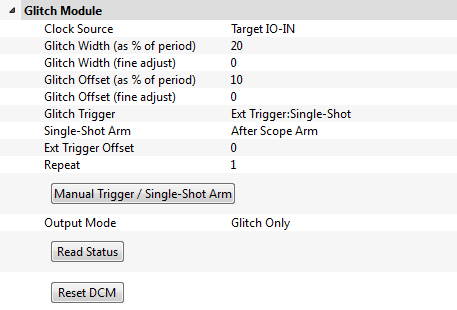
- Make sure the clock source is Target IO-IN
- Set the glitch trigger to Ext Trigger:Single-Shot
- Set the output mode to Glitch Only
- Take a look at the glitch width/offset, the trigger offset, and repeat - feel free to experiment with these throughout the tutorial
Then, in CW Extra Settings, turn on one or both of the HS-Glitch Out Enable checkboxes. These are used to enable low-power and high-power MOSFETs, respectively; we found that the low-power output is powerful enough for this board, but you might see different effects with the different outputs.
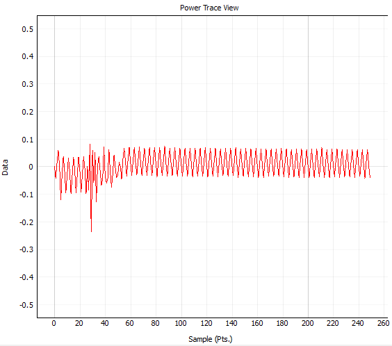
That should be everything. Hit Capture 1 and make sure you see a glitch. This picture was taken with a glitch width of 20%:
From here, you can use the Glitch Explorer to sweep the glitch settings and search for a successful glitch, as we did in Tutorial CW305-3 Clock Glitching. Good luck!
Hints
We had a lot of trouble creating a successful voltage glitch. If you're stuck, this section has a few ideas that you can try.
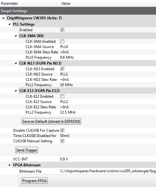
Core voltage: the CW305 board has a programmable power supply with an adjustable output voltage. This voltage level can be modified in the Target Settings tab: the VCC-INT field can be adjusted to any level from 0.6 to 1.1 V.
You might find that your glitch attacks work better when the target is on the edge of its operating limits. For example, we found that our AES implementation stops working when VCC-INT is below 0.75 V, and it was much easier to produce effective glitching with the voltage at this level.
Clock speed: The onboard PLL is also programmable to produce a range of clock frequencies. This setting can be accessed from the same tab as the core voltage - the relevant field is the PLL1 Frequency.
The maximum frequency that the FPGA can use depends on the details of the program's implementation. The internal connections inside the FPGA cause a non-zero amount of delay, and running at very high speeds can cause things to go haywire. Again, you can sweep this setting to find the highest working frequency and try your glitch attacks at the highest working speed to increase your chances of success.
Enable-only glitches: During our tests, we found that the Glitch Only output was too soft - we couldn't get any useful glitches out of this. As an alternative method, you can try the Enable Only output setting. This effectively causes the glitch signal to have a duty cycle of 100%, so the glitch width and offset have no effect. Then, this pulse can be adjusted with the Ext Trigger Offset and Repeat settings. Be warned that this type of glitch is more likely to corrupt the FPGA configuration with its longer pulses!
High-speed glitches: There is one extra trick that can help with the Enable Only output mode. Try the following:
- Make sure that the Artix-7 is being driven by its onboard PLL, not the CLKGEN output.
- Under CLKGEN Settings, change the Input Source to
extclk. Now, the CLKGEN clock will be a multiple of the EXTCLK clock. - Adjust the CLKGEN speed with the Multiply and Divide settings. It might be helpful to use the Frequency Counter here to make sure that the CLKGEN frequency is as fast as you think it is.
- Set up the ADC to use EXTCLK (x1 or x4) as its source - CLKGEN will probably be too fast for the ADC.
- Set the glitch module's clock source to CLKGEN.
Now, you can run the glitch module as fast as you want! This allows for better resolution while working with Enable Only mode: one extra "clock cycle" of glitch output is a much shorter period of time. Make sure that all of the clocks are locked when you're working with this setup, as it's very easy for them to become unlocked.
For reference, we successfully glitched the AES implementation with the following setup:
- CLKGEN running from EXTCLK with Multiply = 8 and Divide = 2
- Glitch module running from CLKGEN with Repeat = 9 and Offset = 0
- Target running at VCC-INT = 0.75 V and PLL1 = 50 MHz


