| As of August 2020 the site you are on (wiki.newae.com) is deprecated, and content is now at rtfm.newae.com. |
Tutorial CW305-1 Building a Project
The CW305 target is an FPGA target board for use with the ChipWhisperer capture hardware. This board lets you test side channel analysis techniques on an Artix-7 FPGA. With this setup, a different toolchain is required: we won't be building C firmware with a makefile. This tutorial walks through the various steps required to run an AES-128 example on the CW305 target.
Contents
CW305 Hardware
If you're used to working with the ChipWhisperer Lite XMEGA or the UFO targets, the CW305 board will feel a bit different. Rather than sending data through a UART directly from the capture hardware, we'll now use two separate connections to the target board.
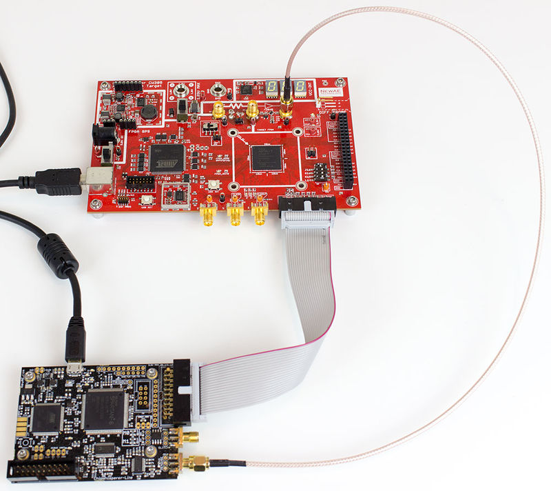
To get started, we need to make three connections to the CW305 target:
- We'll control the Artix-7 directly from the laptop via USB. This is done through the USB-B port on the left side of the board. (On the target, the Atmel SAM3U chip converts these USB packets into signals that the FPGA can understand.)
- We'll get control information for our power measurements through the 20-pin connector at the bottom of the board. This needs to be connected to your capture hardware (a ChipWhisperer Lite or Pro).
- Our power measurements will be done through an SMA cable. Depending on your capture setup, there are three SMA connectors that allow access to the power line in three ways (before the shunt resistor, after the shunt, and after a low noise amplifier). For the ChipWhisperer hardware, we'll connect the third one to our capture board. This provides a nice amplified signal we can pick off.
Using a ChipWhisperer Lite, the full hardware setup looks like:
Target Firmware
In the ChipWhisperer examples, the Artix-7 FPGA is programmed using Verilog. This section describes how to open and build one of these projects. It also describes the layout of the AES-128 example, which is a good starting point for making new FPGA projects.
Note if you just want to follow along with the rest of the tutorials, you can use the pre-built bitstream (.bit file). In which case simply skip ahead to any of the following tutorials.
Opening the Project
The first thing we'll need is Xilinx Vivado HLx, which is their FGPA design software. The fully featured versions of this software require a $3000+ license. However, the WEBPACK version is free, with the limitation that it can only be used with 4 families of devices (including the Artix-7). This is a huge download, so get it started while you read (possibly also you'll have time for lunch and a few drinks).
For this tutorial, a pre-existing AES-128 encryption example is waiting for us deep inside the ChipWhisperer repository. You can find this at chipwhisperer\hardware\victims\cw305_artixtarget\fpga\vivado_examples\aes128_verilog. There are a couple of files and directories here:
-
aes128_verilog.xpris the project file. You can open this project using Vivado. -
aes128_verilog.srcs\contains Verilog source files for the project. Note that most of the code for this project is stored elsewhere - take a look atcw305_artixtarget\fpga\common\andcw305_artixtarget\fpga\cryptosrc\too. -
aes128_verilog.runs\contains the compiled output that is synthesized in Vivado. The most important part of this output is the bitstream (a .bit file), which is what we'll upload onto the target board.
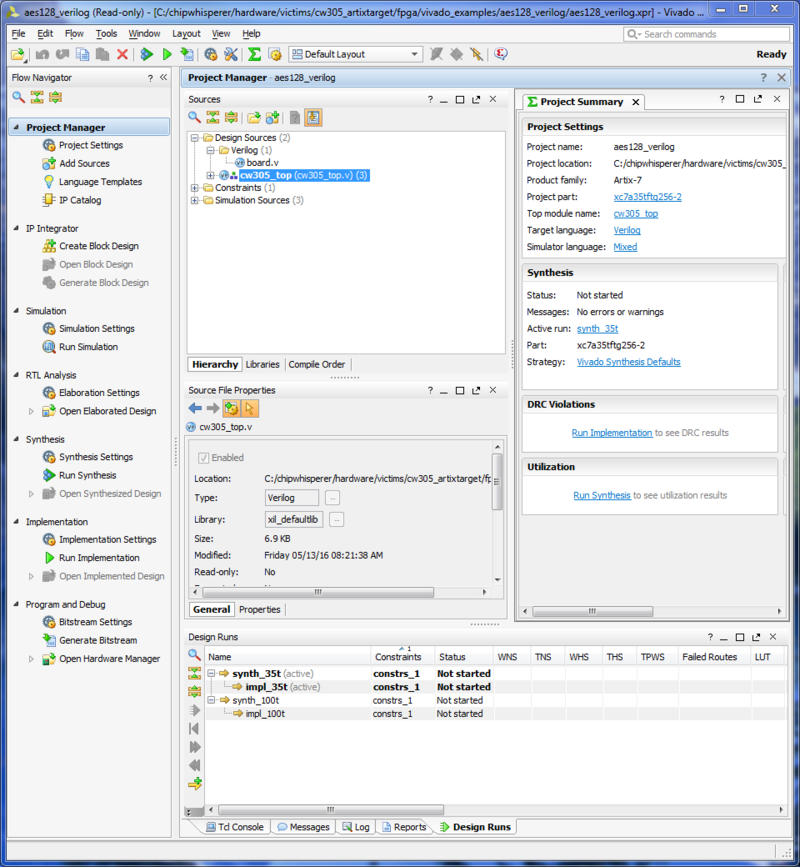
When you open the project file, you should be greeted with a screen like:
This is enough for us to start poking around in the code.
FPGA Code Layout
If you're planning on making your own projects for side channel analysis, it's helpful to understand how the sample project is set up. Here's a high-level description of the different pieces:
-
cw305_main.xdc: The constraints file has a list of pins on the Artix-7 package. It describes how these physical pins are connected to the internal structures on the FPGA. -
cw305_top.v: The top-level module defines all of the ports that are referenced in the constraints file. It connects these ports to the lower level modules. For example, the USB data and address pins are connected to a USB module here. Notably, there are two 1024 byte ports that are shared between the USB module and the register module. -
usb_module.v: The USB module is used to communicate with the Atmel SAM3U microcontroller. It allows the Atmel to access the 1024 byte memory, reading from or writing to various locations in memory. -
registers.v: The registers module is used to place various data into the shared memory, allowing the USB module's reads and writes to affect other modules in the code. It places this data at known, fixed offsets in the memory. For example, reading from address 0x100 allows the Atmel to recover the plaintext from an encryption. -
aes_core.v: The AES core module is an implementation of AES from Google. This is taken from the ProjectVault repository.
Building the Project
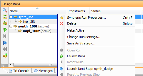
This project is already fully built for us. However, if you want to make your own project, you'll need to know how to build it. There are three steps that Vivado takes to turn our Verilog into a fully functional piece of code:
- Synthesis: the Verilog code is synthesized into a gate-level representation
- Implementation: the synthesized logic is routed to fit onto the device
- Bitstream Generation: an Artix-ready file is created, allowing us to upload our firmware onto the FPGA
This process can take a while - on an average laptop, the sample project takes around 7 minutes to build.
Capture Setup
With our FPGA bitstream in hand, we're now ready to capture a power trace. We can set this up using the ChipWhisperer Capture software.
We'll need to set up the DIP switches on the CW305. These are the four switches next to the 20-pin connector. We need to set two of them for this project:
- J16: 0 - use the on-board PLL to clock the FPGA
- K16: 1 - route the FPGA's clock to the ChipWhisperer's HS-In channel
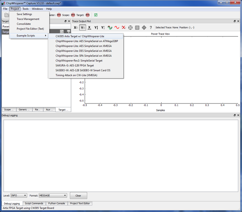
Next, we need to set up the software. To make this process simple, there is an existing sample script that connects to the CW305 using the ChipWhisperer Lite. This script is located in
Project -> Example Scripts -> CW305 Artix Target w/ ChipWhisperer-LiteThis script will connect to the CW305 and ChipWhisperer Lite, setting them up for a capture.
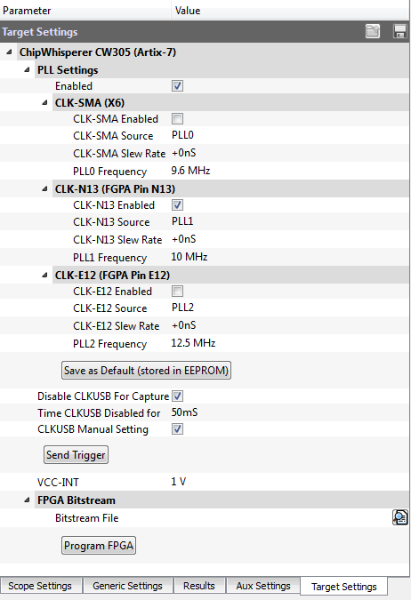
The FPGA bitstream needs to be programmed onto the Artix board. There is a button called "Program FPGA" that takes a bitstream (specified the line above that button) and programs it into the FPGA.
-
Select the bitstream file that we generated earlier (
chipwhisperer/hardware/victims/cw305_artixtarget/fpga/vivado_examples/aes128_verilog/aes128_verilog.runs/impl_35t/cw305_top.bit) and program it onto the FPGA. If using the 100T size FPGA, you will find the file in a directory labeled impl_100t instead.NOTE: Even if you haven't completed the build portion, you can simply use the pre-built bitstream!
-
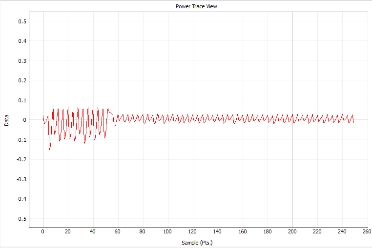
Now, the Capture 1 button should give us a short and sweet power trace:
Success! We've built a project and recorded a power trace using the Artix target.
For further analysis using this project, check out the next tutorial: Tutorial CW305-2 Breaking AES on FPGA.
