| As of August 2020 the site you are on (wiki.newae.com) is deprecated, and content is now at rtfm.newae.com. |
Difference between revisions of "CW301 Multi-Target"
| (One intermediate revision by one other user not shown) | |||
| Line 1: | Line 1: | ||
| − | {{ | + | {{Warningbox|As of August 2016, this product is now end-of-life. No new units will be available for sale except for special order with minimum order quantity applying. Instead we are focusing on the [[CW308 UFO Target]]. The design files for this board are available in the GIT repository. This page will not be updated. }} |
= CW301 Target: MultiTarget Victim Board = | = CW301 Target: MultiTarget Victim Board = | ||
| Line 284: | Line 284: | ||
[[File:Multitarget_lna.jpg|frame|none]] | [[File:Multitarget_lna.jpg|frame|none]] | ||
| + | |||
| + | == Hardware == | ||
{{Template:Hardware}} | {{Template:Hardware}} | ||
[[Category:Targets]] | [[Category:Targets]] | ||
Latest revision as of 11:30, 1 May 2018
As of August 2016, this product is now end-of-life. No new units will be available for sale except for special order with minimum order quantity applying. Instead we are focusing on the CW308 UFO Target. The design files for this board are available in the GIT repository. This page will not be updated.
Contents
CW301 Target: MultiTarget Victim Board
Layout of the Board
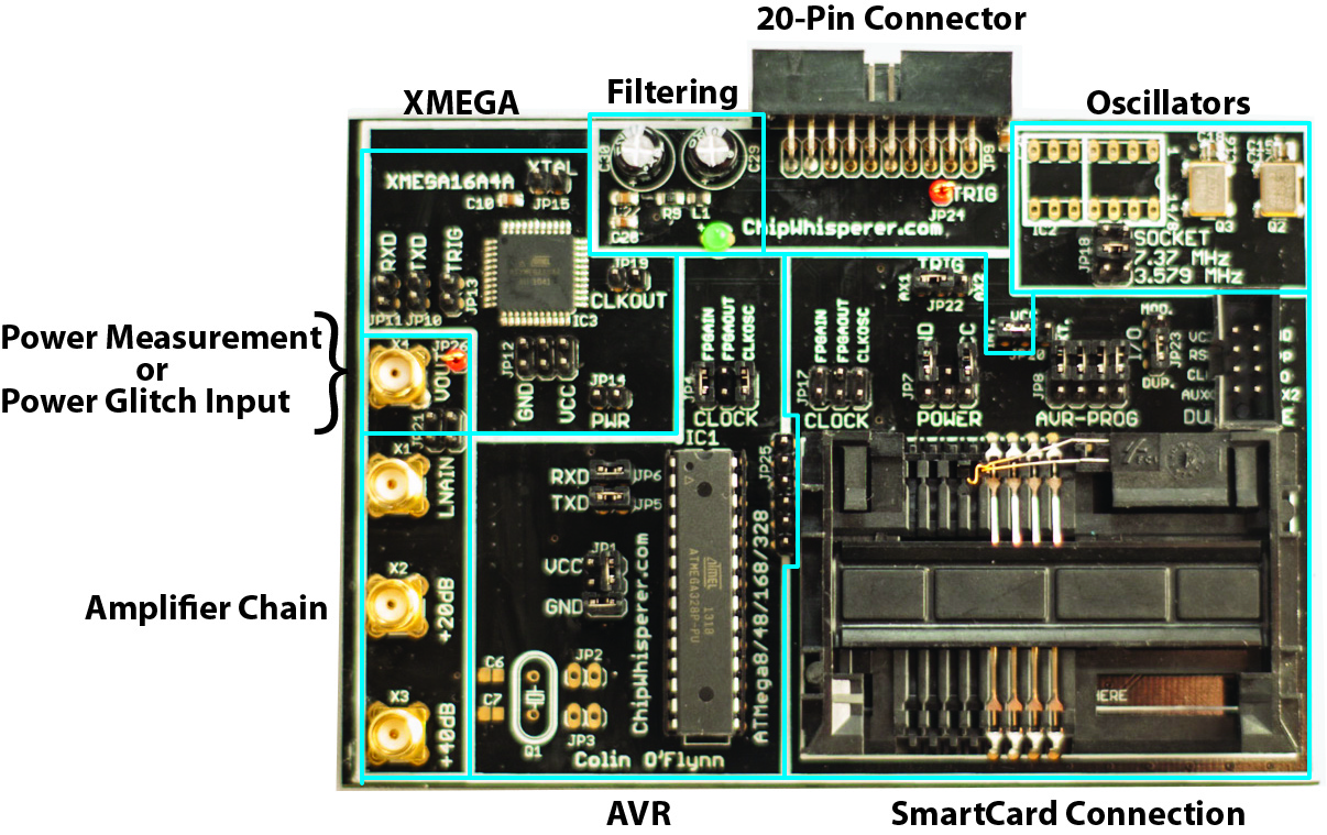
The general board layout is shown in the following image:
Specifics of each section will be discussed next.
The 6-Pin Headers
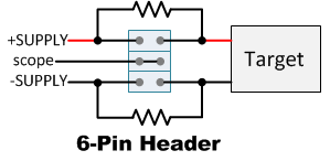
A core feature of the MultiTarget board is the 6-pin shunt header, allowing you to select choice of shunt type, noise measurement, differential measurement, and glitch injection. The layout of the 6-pin header is typically as follows, but be aware that VCC & GND may be swapped, see the silkscreen on the PCB:
Using a jumper, you can measure the noise on the VCC or GND line for example:
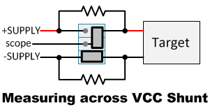
Or select to measure the power across either the VCC or GND shunts:
The above figures can also be used for glitch injection - the 'scope' line is connected to a pulse generator. The shunt resistor will allow driving of glitches onto the power supply rails of the chip, and the shunt resistor will simply appear as a standard 50-ohm termination of the pulse generator output.
warningBe sure to only attach a jumper to a SINGLE target on the multi-target board. This can otherwise cause serious problems as some parts are 3.3V only, and some parts have the ability to handle 5V supplies. This warning will be highlighted again when looking at the jumper selection for the SmartCard device.
Target Voltage Selection
The target devices are typically 3.3V only, however the smartcard socket can operate at 5V when running in pass-through mode. To accomplish this the 'VREF' pin is set to the operating voltage of the targets, and all IO lines (e.g. the serial data lines) will have correct voltage-levels for the specific target.
JP20 selects the IO standard in use. Typically this should be set to INT., which will use 3.3V standards. If operating the smartcard in pass-through mode it might be needed to set this to EXT., see the section #Smartcard_Target_Section.
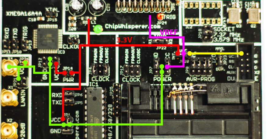
The following figure shows the routing of power. Pay careful attention to the fact that the 'VOUT' measurement is routed to ALL targets. Thus when you are not using a target, you MUST remove the jumpers on the 6-pin shunt selection header. If you fail to do this, you will at minimum add additional noise. However it's also possible to shunt the device supplies together if e.g. you shunt the 'EXT' supply from the SmartCard onto the 3.3V supply for the AVR.
warningBefore selecting EXT. for JP20, ensure jumpers are removed from the AVR & XMEGA target zone. Pay careful attention to ensure jumpers JP1 and JP12 are clear. It is possible to short the 5V rail onto the 3.3V rail by incorrect use of the jumpers, which may destroy your ChipWhisperer Device (e.g. NOT just the target board, but the entire hardware).
Oscillator Selection & Net
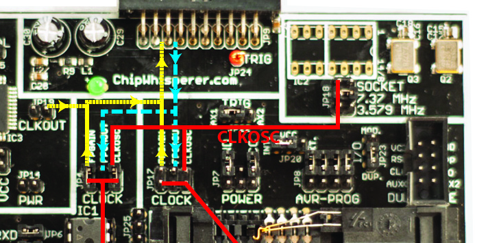
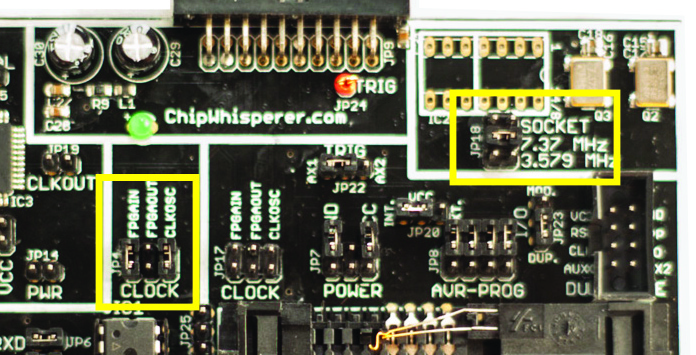
By default, the board ships with a 7.3728 MHz and 3.579 MHz crystal oscillator. These devices are capable of generating a 3.3V logic-level oscillator signal. There is also a DIP pinout, which you could mount a standard 8-DIP or 14-DIP sized oscillator onto. The oscillator section is shown below, where a series of jumpers can connect these oscillators to the CLKOSC net.
The AVR target and SmartCard target have local clock networks you can choose to connect the correct clock source to. Normally the usage of these jumpers is to route an oscillator of choice (7.37MHz for AVR, 3.579MHz for SmartCard) to the local clock network. This local clock network is also routed back to the FPGA. The following shows such an example for the DIP AVR, although similar settings could be used on the SmartCard:
The clock output from the FPGA is used when generating a clock on the FPGA, or for clock glitching. Thus in most normal cases the FPGAOUT is not used.
The XMEGA has differing setup of clock selection, which is described in more detail in the XMEGA Specific section.
20-Pin Target Header
The 20-pin target header can connect to the ChipWhisperer Hardware, a breakout board, or the Papilio Pro adapter. The 20-pin header has the following pinout:
| Number | Name | Dir | Description |
|---|---|---|---|
| 1 | +5V | N/C | Not Connected |
| 2 | GND | I | System GND. |
| 3 | +3.3V | I | +3.3V Power Supply |
| 4 | FPGA-HS1 | I | Clock input to Target Board (connected to FPGAIN) |
| 5 | PROG-RESET | I | Target RESET Pin (AVR Programmer). |
| 6 | FPGA-HS2 | O | Clock output from Target Board, connected to FPGAOUT. |
| 7 | PROG-MISO | O | MISO for AVR Programmer. |
| 8 | VTarget | O | Connected to JP20 'IO VREF', normally 3.3V but can vary for SmartCards. |
| 9 | PROG-MOSI | I | MOSI for AVR Programmer. |
| 10 | FPGA-TARG1 | I/O | TargetIO Pin 1 - Usually UART RX. |
| 11 | PROG-SCK | I | SCK for AVR Programmer. |
| 12 | FPGA-TARG2 | I/O | TargetIO Pin 2 - Usually UART TX. |
| 13 | PROG-PDIC | I | PDI Programming Clock (XMEGA Programmer) |
| 14 | FPGA-TARG3 | I/O | TargetIO Pin 3 - Usually bidirectional IO for smartcard. |
| 15 | PROG-PDID | I/O | PDI Programming Data (XMEGA Programmer). |
| 16 | IOTarget4 | O | Trigger Output |
| 17 | GND | I | |
| 18 | +3.3V | I | |
| 19 | GND | I | |
| 20 | +5V | N/C | Not Connected |
warningYou do not need to connect +5V, it is unused in this target normally. Only apply 3.3V to the 3.3V rail, as a number of parts such as the LNA chips are only rated to a maximum of 3.3V. The VREF pin is an output here who's value is set by JP20, do not drive this pin. If using the breakout board do not mount the voltage selection jumper.
AVR Target Section
A 28-pin DIP socket can hold one of the following AVRs: AtMega8, AtMega48, AtMega88, AtMega168, and AtMega328P. Note that many of these devices are available in various 'flavours' such as the AtMega88A or AtMega88P, which are pin-compatible and effectively the same for our application. Some information on this target:
- The AVR is always powered from the 3.3V supply. When using the AVR it is critical that jumper JP20 is set to INT. so that the IO standard is set to 3.3V.
- IC1 is the 28-pin DIP socket for the AVR
- JP1 is the standard 6-pin power selection header, described in 6pin.
- *; JP6 and JP5 are the connection to the USART on the AtMega328P device.
- *;* JP5 connects to pin PORTD.0, which is the RXD (input) on the AVR.
- JP6 connects to pin PORTD.1, which is the TXD (output) on the AVR.
- When not using the AVR remove these jumpers to isolate the AVR from the shared serial connections.
- JP4 is the clock selection jumper, explained in #Oscillator_Section_.26_Net.
- JP2, JP3, Q1, C6, and C7 can be used to mount an external crystal and connect to the XTAL pins on the AVR
Triggering Notes
All external trigger lines use the PORTC port, which is also the ADC. This is done because the digital drivers for PORTC actually come from the AVCC pin and not the VCC pin. Thus any transitions on the PORTC lines do not generate as large a spike in the power measurements compared to similar transitions on PORTB/PORTD.
- The trigger line is connected to PORTC.0, and there is no jumper to isolate it. If using another target you must remove the 28-pin AVR from the socket.
JP25 is the extra connection pins, which connect to PORTC and are also the ADC inputs to the AVR. 'Pin1' on JP25 is the top-most pin (e.g. closest to JP17), and the mapping of those pins is:
JP25 Pin AVR Pin 1 PORTC.1 2 PORTC.2 3 PORTC.3 4 PORTC.4 5 PORTC.5 6 GND
Programming Notes
- The AVR In Circuit Programming (ISP) pins are always connected to the ISP connections (MOSI/MISO/SCK/RESET) on the 20-pin header. If you wish to program the 28-pin DIP, ensure that all jumpers on JP8 are removed. If you wish to program the SmartCard, you need to remove the 28-pin AVR from the socket, as there is no way to isolate the programming lines of the 28-pin DIP except for removing the device.
Warnings
warningYou MUST set jumper JP20 to INT. to ensure the IO standards on the RXD and TXD lines are 3.3V.
warningWhen using another target than the AVR, you must remove the IC from the socket, as there is no way to isolate the trigger. In addition be sure to also clear the 6-pin shunt selector (JP1). Clearing JP1 is to protect the board and NOT to protect the AVR (which is no longer present anyway). Do not forget to clear JP1 when removing the AVR.
XMEGA Target Section
An ATXMEGA16A4 device is mounted on the target board. Note that since the device is soldered down, jumpers are provided which are able to electrically isolate the device from the rest of the board when you are not using the XMEGA. Some notes on the XMEGA device:
- The XMEGA is always powered from the 3.3V supply. When using the AVR it is critical that jumper JP20 is set to INT. so that the IO standard is set to 3.3V.
- JP12 is the 6-pin shunt selection jumper, note that JP14 is needed to power up the JP12 jumper.
- *; JP11 and JP10 are the connection to the USART on the XMega device.
- *;* JP10 connects to pin PORTC.2, which is the RXD (input) on the XMEGA.
- JP11 connects to pin PORTC.3, which is the TXD (output) on the XMEGA.
- When not using the AVR remove these jumpers to isolate the AVR from the shared serial connections.
- JP13 is the 'Trigger' connection on the XMEGA, which connectors to PORTA.0. This is one of the analog pins as well.
- JP19 connects pin PORTD.7 to the FPGAIN clock network. PORTD.7 is the output pin from the XMEGA so you can synchronize to the internal RC oscillator.
- JP15 is the two XTAL/CLK pins on the XMEGA. If you want to route an external clock to the XMEGA, you can do so by running a jumper wire from a suitable source (e.g. one of the FPGAOUT pins or the oscillators) to the XMEGA.
- Using the 'CLKOUT' net from the XMEGA seems to cause excessive noise on the shunt resistor, which causes analysis to fail. It's recommended to jumper the clock oscillator into the XTAL1 pin on JP15. Future revisions of this board will have a clock jumper to simplify this.
The XMEGA is programmed via the PDI interface, and the PDI pins on the XMEGA connect to the 20-pin target header.
warningThe XMEGA is a 3.3V only device. Always remove ALL jumpers from the XMEGA section when not using the device, as there can be a somewhat complicated connection of jumpers. It is not sufficient to just remove the 'PWR' jumper for example.
warningEnsure JP20 is set to INT. so that the serial bus lines will drive a 3.3V logic level when using the XMEGA.
SmartCard Target Section
TODO
Pass-Thru/SASEBO-W Adapator
warningIt is completely possible to use the EXT. IO voltage, allowing the ChipWhisperer to interface with 5V SmartCards. Before doing this follow all warnings in #Target Voltage Selection, or you may DESTROY THE CHIPWHISPERER DEVICE by shunting the external power supply onto internal 3.3V rails.
For more details see Sasebo-w#Connecting_the_Multi-Target_Board_to_the_SASEBO-W.
Low Noise Amplifier
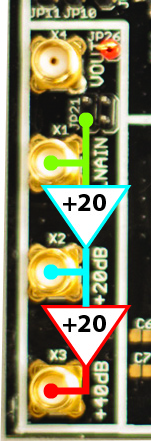
Two 20dB Low Noise Amplifiers (LNA) are mounted on the board. When connecting to standard oscilloscopes, they can be used to amplify very small signals coming from a shunt resistor or H-Field probe.
The LNA chain is shown in the following figure:
