| As of August 2020 the site you are on (wiki.newae.com) is deprecated, and content is now at rtfm.newae.com. |
Difference between revisions of "CW305 Artix FPGA Target"
| Line 2: | Line 2: | ||
This board requires an external oscilloscope or capture box for performing the power measurement. The board is designed to interface to hardware such as the ChipWhisperer-Lite 2-Part version or the CW1200 (ChipWhisperer-Pro). | This board requires an external oscilloscope or capture box for performing the power measurement. The board is designed to interface to hardware such as the ChipWhisperer-Lite 2-Part version or the CW1200 (ChipWhisperer-Pro). | ||
| + | |||
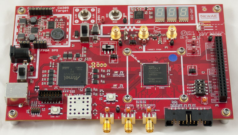
| + | [[File:Artix_Board.jpg|800px]] | ||
=Feature Overviews= | =Feature Overviews= | ||
Revision as of 06:18, 17 January 2017
The CW305 is a FPGA target board. It brings features including a simplified USB interface for talking to the FPGA, an external PLL for adjusting frequency response, a programmable VCC-INT supply, and diode protection for use in fault injection environments. Also available with a special BGA socket, giving you the ability to perform tests on multiple FPGA devices - perfect for checking Physically Unclonable Functions (PUFs) under the exact same environmental conditions across multiple FPGAs.
This board requires an external oscilloscope or capture box for performing the power measurement. The board is designed to interface to hardware such as the ChipWhisperer-Lite 2-Part version or the CW1200 (ChipWhisperer-Pro).
Contents
- 1 Feature Overviews
- 2 Hardware Details
- 3 Software Details
- 4 FPGA Projects
- 5 Example Attacks
- 6 Ordering Options
- 7 Schematic
Feature Overviews
USB Interface
This board uses NewAE Technology Inc's custom USB interface firmware. This firmware gives you a simple data/address bus, which you can read/write to the FPGA. The USB chip also controls FPGA configuration (which for the 7A35T device takes just under 2 seconds), the PLL, and the VCC-INT regulator. This makes it easy to script complex jobs like performing measurements at different frequencies or voltages, or reconfiguring the FPGA after a fault attempt to avoid issues with SRAM corruption.
PLL
The CDCE906 PLL means you can easily output frequencies from about 5-160 MHz (a larger range is possible but may require more care). The PLL is programmed over USB, and 3 output channels are provided (each which can be set to a different frequency). 2 route to the FPGA and 1 routes to a SMA connector. This allows you to synchronize external devices or boards to the oscillator driving your FPGA design.
Power Supply
Three switching regulators are provided - two fixed for VCC-AUX and VCC-IO, along with a VCC-INT supply which can be programmed over the range of 0.8V-1.10V (this is a software limit to prevent you from damaging the FPGA, this can be overridden if you need to provide about a 0.65-1.5V range). Optional linear regulators can plug into the VCC-AUX and VCC-IO supplies which provide lower-noise operation (but with a reduced current limit compared to the switching supplies).
External banana connectors make is simply to power the VCC-INT from a low-noise bench supply. This can improve side-channel analysis measurements by reducing noise in the shunt measurement compared to the on-board switching supply.
An on-board DMM measures the VCC-INT supply and provides easy visual feedback so you can confirm settings without needing to attach a meter.
Shunt Measurement
A resistive shunt is provided in the VCC-INT supply, with an optional shunt in the VCC-AUX line. The resistive shunt can be measured using a differential probe on 0.1" spacing, using the SMAs, or using the on-board 20dB LNA. The LNA makes it easier to measure with standard oscilloscopes that don't measure the very small variations you find in power analysis.
Fault Injection
This board is designed to facilitate all forms of fault injection. Resitive and diode protection prevents transients on the VCC-IO of the FPGA from affecting the USB interface chip. The USB chip itself provides high-speed FPGA reconfiguration to simplify repetitive fault attacks where you need to reconfigure the FPGA. The USB interface can also monitor the INITB pin of the FPGA, which can be used with the continous CRC verification feature to determine when reconfiguration is required.
The PCB features mounting holes and alignment features for use with an X-Y table (suitable for both EM fault injection and H-Field probes).
The VCC-INT supply can be disconnected from the filtering capacitors to allow using the SMA jacks as a method of inserting voltage faults without fighting the output capacitance of the power supply.
The ChipWhisperer Crowbar fault injection can also be used with this board, which requires either the ChipWhisperer-Lite 2-Part version (CW1173-2PART) or CW1200.
Hardware Details
VCC-INT Routing
The following shows details of how the power supplies are routed on the CW305 board:
Details of each section are shown here:
DC Jack / USB Power
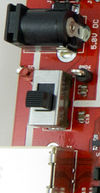
There are two main sources of power which can be used for all FPGA power supplies (VCC-INT, VCC-IO, and VCC-AUX). By default this is the USB connector, but this is limited by USB specs to a maximum of 500 mA.
If using a larger design in the FPGA you may exceed these limits, in which case you must move the switch to use the DC-Jack. This jack requires a 5.0V power supply capable of a suitable amount of current for your design (suggested: 2.0A).
Internal / External VCC-INT
The internal power supply provides a source of 1.0V for the VCC-INT. This supply can be programmed slightly above/below 1.0V to compare the effects of different VCC-INT supplies on the FPGA design. Details of the power supply are given in section TODO XREF. The internal supply can provide up to 6.0A for the VCC-INT rail.
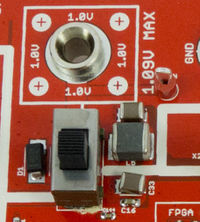
There is also two banana jacks which can be connected to a 1.0V lab supply. You must be very careful to ensure you do not exceed 1.10V on this input, as beyond that range you risk damaging the FPGA.
The choice of internal/external is selected with the switch. There is a ferrite bead + large capacitors after this switch, so note that you cannot use the banana jack inputs as a voltage glitch insertion method. Instead you must insert them directly into the SMA connectors, described later.
Shunt Resistor Connections
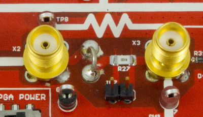
The following shows the components around the shunt resistor:
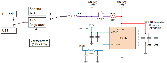
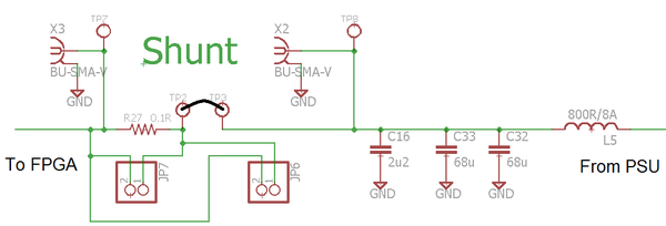
Schematically, this is shown below. NOTE: the schematic flows in the "opposite" direction of the PCB. In the PCB power flows left to right, in the schematic it flows right to left.
A brief description of each element is given below.
SMA Connectors / Test Points
The SMA connectors provide access to both sides of the shunt. The "high side" comes from the power supply with substantial filter capacitors, and the "low side" goes directly to the FPGA VCC-INT network. The VCC-INT network may or may not have decoupling capacitors mounted (this is an ordering option).
In addition, two test points are provided on each side that are suitable for use with an oscilloscope probe. It is strongly recommended to use a SMA to BNC cable (such as Cinch Connectivity P/N 415-0028-024 available from Digikey) to view the power measurement instead of these test points, as the SNR of the oscilloscope probe will typically be considerably worse than via the SMA connector.
The SMA connector can also be used when inserting faults into the FPGA. If using the ChipWhisperer crowbar fault generator, simply connect the crowbar output to connector X3. If using an external fault amplifier, you will also connect to X3 but will also need to remove the jumper (described below).
Jumper
In some circumstances you may wish to entirely remove the shunt resistor. This is typically the case when performing fault insertion, where the large "filter" capacitors present on the high side of the shunt resistor will drastically reduce the slew rate of your fault amplifier.
Alternatively, you may wish to use a current transformer or similar current probe which requires a method of inserting a sensor into the VCC-INT path.
For these uses test point TP2 and TP3 have gold-plated "nails" soldered into them, and a wire bridge soldered between the test points. This wire bridge can be removed by either cutting (with wire cutters) or desoldering. The gold-plated nails provide a mechanically strong base which allows you to perform this operation without risking damage to the CW305 PCB.
If using a current probe, you can either (1) solder a wire between TP2 and TP3, or (2) use two SMA connectors to route the power between X2 and X3. Clamp your current probe onto the bare wire used to route the signal between these (you'll need a custom cable without the shield most likely).
The gold-plated nails that require soldering are used instead of a switch or jumper to reduce the resistance in the measurement path. Typical switches provide too high of a contact resistance for the potential current draw of a large design in the FPGA, which would reduce the SNR at the measurement point.
Shunt Resistor
The shunt resistor is a 1206 size resistor mounted at position R27. The value of this resistor will vary between the various variants of the assembled board.
Two 0.100" (2.54mm) headers are provided for measurement with a differential probe. One (JP7) is directly across the resistor, and the other (JP6) is on the top right side of the PCB. JP6 is designed to be used with a NewAE Technology Inc. differential probe (which requires a separate power supply for this differential probe).
Examples of resistors used are the following:
| Value | Manufacture | Part Number | Digikey P/N |
|---|---|---|---|
| 500mOhm | Stackpole | CSR1206FKR500 | CSR1206FKR500CT-ND |
| 250mOhm | Stackpole | CSR1206FKR250 | CSR1206FKR250CT-ND |
| 100mOhm | Samsung | RUW3216FR100CS | 1276-6187-1-ND |
| 50mOhm | Vishay | WSLP1206R0500FEA | WSLP-.05CT-ND |
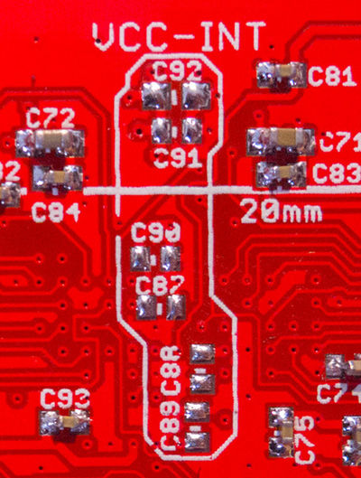
VCC-INT Decoupling Capacitors
The optional decoupling capacitors for the VCC-INT rail are shown on the underside of the PCB here:
This capacitors are typically not mounted when using the shunt resistor to measure power waveforms.
VCC-AUX Shunt Resistor
The VCC-INT shunt is the primarily power measurement point, as it provides power measurement for both designs inside the FPGA, along with the logic responsible for decrypting bitstreams (as reported at https://eprint.iacr.org/2016/249.pdf).
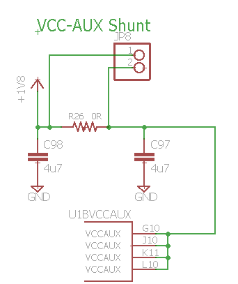
There may be additional information in the VCC-AUX power supply however, for example monitoring JTAG state transitions. There is a secondary shunt position (by default with no shunt mounted) for exploration of the VCC-AUX power supply. This can be seen in the schematic here:
The shunt is located on the rear side of the PCB, as shown here:
If using this shunt, you must remove resistor R26 (which has a metal slug 0-ohm resistor mounted) and replace with an appropriately sized 0805 resistor (suggested: 1 ohm). You must also remove capacitor C98, C95, C97, C94, and C93. They can be seen in the above photo.
On-Board Power Supplies
Three switching power supplies are present on the board, which provide the VCC-INT (1.0V), VCC-AUX (1.8V), and VCC-IO (3.3V) supplies. The external IO on the board are all operated at 3.3V.
Power Supply Source
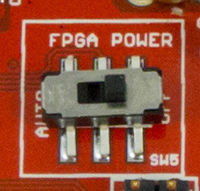
You can turn the power to the FPGA on or off using the following switch:
When in the "OFF" mode the VCC-INT, VCC-IO, and VCC-AUX supplies are turned off. In addition the communications interfaces are all disabled to avoid back-powering the FPGA via the IO pins. If you have external connections (such as driving a clock from the ChipWhisperer) you need to ensure they are also disabled when the power is turned off.
When in the "AUTO" mode, the state of the power supplies can be controlled from the computer. Typically "AUTO" mode is used as it allows the computer to power cycle the device.
Low-Noise Power Supplies
Optional low-noise linear power supplies are available, which fit into the connectors around the switch-mode power supply. They have less power handling capabilities than the on-board switch-mode supplies, but have reduced noise that ends up injected into the PCB (and thus on the power traces).
These power supplies are only used for VCC-IO and VCC-AUX. Like the on-board supplies they will be disabled when the power to the FPGA is switched off using either the API interface or the target power switch.
If you wish to have the lowest-noise power source, you must mount the VCC-IO and VCC-AUX low-noise supplies, and also use an external supply for the VCC-INT supply.
Shunt Selection
Fault Injection
IO Connections
The board contains a number of additional headers.
GPIO Header
A 40-pin header is mounted at JP3. This female header also comes with a dual-sided male 40-pin header which ships which each PCB, allowing you to use either gender of connectors with this header.
The pinout of the header is marked on the PCB. All pins are routed to 3.3V VCC-IO banks on the Artix 7 FPGA. The layout of the header is such that the following can directly be plugged into the board:
- Digilent Inc PMOD devices
- NewAE OpenADC Module
20-Pin ChipWhisperer Connector
The bottom right side of the PCB contains a 20-pin connector that follows the standard ChipWhisperer pinout. This connector has ESD diodes present on the PCB to protect both the FPGA from external transients, and from glitches inserted into the FPGA from exiting the board and damaging external test gear.
LEDs
SMA Connectors
Three SMA connectors are present on the board. Two are routed to IO pins on the FPGA, and one routes directly to the on-board PLL.
Switches
Two user switches are provided: one push-button, and one 4-item DIP switch.
The push-button (SW4) routes to FPGA pin R1.
The dip-switch (S2) routes to FPGA pins J16, K16, K15, and L14 (see PCB silkscreen). With generic designs that dip-switch has the following uses:
| J16 | Input Clock Source |
|---|---|
| 1 | ChipWhisperer HS-IO |
| 0 (Default) | PLL1 |
| K16 | ChipWhisperer HS-Out |
|---|---|
| 1 (Default) | Enabled (clock) |
| 0 | Disabled |
See the example design documentation for more details.
FPGA Configuration
There are three modes you can use to configure the FPGA:
1. Over USB using ChipWhisperer software. Requires reconfiguration on every power cycle.
2. Over JTAG from Xilinx software. Requires reconfiguration on every power cycle.
3. From on-board SPI-Flash on power-up.
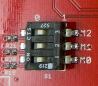
These modes are selected by different FPGA mode switch settings. The mode switches are on the back-side of the PCB as shown below. Note if the switch is set to the left the mode bit is "0", and if the switch is set to the right the bit is set to "1". The mode bits themselves are labeled M2, M1, and M0 from top to bottom.
The setting of the mode switches must be set as in the following table for the desired configuration mode:
| M0 | M1 | M2 | Configuration Mode |
|---|---|---|---|
| 1 | 0 | 0 | SPI Flash |
| 1 | 0 | 1 | JTAG |
| 1 | 1 | 1 | USB (Default) |
Software Details
The ChipWhisperer software is used to communicate with this board. This can be used either as part of the GUI (i.e., using the CW305 within the ChipWhisperer-Capture), or by importing Python modules and communicating with the CW305.
Driver and Software Installation
Windows Drivers
Signed Windows drivers are provided in the GIT repository, or can be downloaded from here. To install drivers:
- If you don't have a clone of the GIT repository, download & unzip the zip-file somewhere.
- Plug the USB cable in, and once Windows detects the board you will be able to point it to a folder with drivers. Point it to either (a) the unzipped folder if you downloaded drivers, or (b) the folder
/chipwhisperer/hardware/victims/cw305_artixtarget/usb_driver/if using the GIT repository.
Note you can also try using the installer present in this folder, but it's suggested instead to point the Windows installer to the driver folder.
Linux Drivers
If you have previously setup the CW-Lite or CW-1200 on Linux, you should already have a rules.d file with some NewAE products. You can add the following to get the CW305 working:
# allow users to claim the device
SUBSYSTEM=="usb", ATTRS{idVendor}=="2b3e", ATTRS{idProduct}=="c305", MODE="0664", GROUP="plugdev"
If you haven't previously set this up, see the page Linux Driver Setup for details.
Python Example
Connecting and Programming
You can connect to the board using the following command:from chipwhisperer.capture.targets.CW305 import CW305
cw = CW305()
cw.con(bsfile=r"C:\chipwhisperer\hardware\victims\cw305_artixtarget\fpga\vivado_examples\aes128_verilog\aes128_verilog.runs\impl_35t\cw305_top.bit", force=False)
If doing development, you probably want to set the force flag to "True". This will ensure you always get a newly programmed FPGA with the latest bitstream.
Running AES-128 Example
You can run the AES-128 example code (the cw305_top.bit file) with the following example:from chipwhisperer.capture.targets.CW305 import CW305
cw = CW305()
cw.con(bsfile=r"C:\chipwhisperer\hardware\victims\cw305_artixtarget\fpga\vivado_examples\aes128_verilog\aes128_verilog.runs\impl_35t\cw305_top.bit", force=False)
test_key = [0x2b, 0x7e, 0x15, 0x16, 0x28, 0xae, 0xd2, 0xa6, 0xab, 0xf7, 0x15, 0x88, 0x09, 0xcf, 0x4f, 0x3c]
test_inp = [0x6b, 0xc1, 0xbe, 0xe2, 0x2e, 0x40, 0x9f, 0x96, 0xe9, 0x3d, 0x7e, 0x11, 0x73, 0x93, 0x17, 0x2a]
exp_result = [0x3A, 0xD7, 0x7B, 0xB4, 0x0D, 0x7A, 0x36, 0x60, 0xA8, 0x9E, 0xCA, 0xF3, 0x24, 0x66, 0xEF, 0x97]
cw.loadEncryptionKey(test_key)
cw.loadInput(test_inp)
cw.go()
result = cw.readOutput()
print "ACT: "+" ".join(["%02X"%c for c in result])
print "EXP: "+" ".join(["%02X"%c for c in exp_result])
from chipwhisperer.capture.targets.CW305 import CW305
import random

cw = CW305()
cw.con(bsfile=r"C:\chipwhisperer\hardware\victims\cw305_artixtarget\fpga\vivado_examples\aes128_verilog\aes128_verilog.runs\impl_35t\cw305_top.bit", force=False)

test_key = [0x2b, 0x7e, 0x15, 0x16, 0x28, 0xae, 0xd2, 0xa6, 0xab, 0xf7, 0x15, 0x88, 0x09, 0xcf, 0x4f, 0x3c]

plaintexts = []
ciphertexts = []

for tnum in range(0, 20):
    pt = [random.randint(0, 255) for i in range(0, 16)]
    cw.loadEncryptionKey(test_key)
    cw.loadInput(pt)
    cw.go()
    ct = cw.readOutput()

    plaintexts.append(pt)
    ciphertexts.append(ct)

    print "result %d:"%tnum
    print " pt: " + " ".join(["%02x"%d for d in pt])
    print " ct: " + " ".join(["%02x"%d for d in ct])

#Example - saving to text
ptfile = open("plaintexts.txt", "w")
ctfile = open("ciphertexts.txt", "w")
for i in range(0, len(plaintexts)):
    ptfile.write(" ".join(["%02x"%d for d in plaintexts[i]]) + "\n")
    ctfile.write(" ".join(["%02x"%d for d in ciphertexts[i]]) + "\n")

ptfile.close()
ctfile.close()

#Example - saving to MATLAB workspace
import scipy.io
scipy.io.savemat('pt_ct_mat', {'plaintexts':plaintexts, 'ciphertexts':ciphertexts, 'key':test_key})
Accessing FPGA Registers
See the FPGA Projects section for important details of the FPGA design framework.
Turning off USB Clock & Triggering the FPGA
You can disable the USB interface clock (i.e., the clock used by Address/Data lines). Generally this is recommended during the power measurement, as a separate clock is provided for clocking the cryptographic module. The clock can be turned off with:
cw.usb_clk_setenabled(False)
This will reduce noise in the power measurement.
Once the USB clock is off, you must use a special trigger IO pin (since the address/data interface is disabled). This trigger pin can be toggled to trigger your cryptographic core, rather than relying on a register in your FPGA design.
A complete example of a power measurement might look like this:
#arm scope here
cw.usb_clk_setenabled(False)
cw.usb_trigger_toggle()
#wait for scope to complete here
cw.usb_clk_setenabled(True)
You may wish to add a small delay (such as {time.sleep(0.05)}) after turning off the clock.
You may also need to add a delay after triggering the pin - you don't want to turn the clock back on right away, but depending on your scope module it may report the trigger event has occurred before the capture is complete.
Setting PLL Frequency
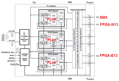
The CW305 contains a 3-channel PLL. This is provided by a CDCE906 chip, which as the following routing diagram shows contains an extremely flexible architecture:
In the software, PLL1 and PLL2 are fixed to FPGA pins N13 and E12 respectively. The SMA output connector X6 can be connected to any of the PLLs (PLL0, PLL1, PLL2). This allows you to get a phase-matched clock on X6 that corresponds perfectly with a clock being fed to the FPGA. Due to the relative complexity of the PLL architecture, it's recommended to use an indirect API call method described below:
You can use the ChipWhisperer-Capture GUI to control the board, and translate your commands there into commands fed into the API. Doing this requires looking at the "Scripting Output" window. For example when performing a certain series of actions, the following might be printed to the window:
['Target Settings', 'ChipWhisperer CW305 (Artix-7)', 'PLL Settings', 'CLK-SMA (X6)', 'PLL0 Frequency', 15000000.0]
['Target Settings', 'ChipWhisperer CW305 (Artix-7)', 'PLL Settings', 'CLK-SMA (X6)', 'CLK-SMA Enabled', True]
The middle part of the command identifies the parameter being modified, which you can use with
findParam() to identify the specific parameter to modify, and the last value specifies what you should send to setValue(). For example the following would be the associated Python code you could use with the cw object based on the above two lines:cw.findParam(['PLL Settings', 'CLK-SMA (X6)', 'PLL0 Frequency']).setValue(15000000.0)
cw.findParam(['PLL Settings', 'CLK-SMA (X6)', 'CLK-SMA Enabled']).setValue(True)
findParam() and setValue()) is the recommended way of interacting with the Python object, as it allows you to first use the GUI to get the desired response, and then directly copy those actions into a code block. Interacting directly with the API requires more knowledge of the underlying PLL architecture.
Optionally, you can directly access the PLL object at cw.pll - this allows complete control of routing options (beyond what is exposed in the more basic API). You can see the source file at chipwhisperer/hardware/naeusb/pll_cdce906.py for details.>>> cw.pll
<chipwhisperer.hardware.naeusb.pll_cdce906.PLLCDCE906 object at 0x068CBDD0>
Setting VCC-INT
You can adjust the VCC-INT voltage using the following command:
#Set vcc-int to 0.95V
cw.vccint_set(0.95)
Turning Power On/Off
In addition to adjusting the VCC-INT supply, you can power cycle the FPGA target section. This can be used when you might expect faults to occur (such as after performing a glitch attack), where you want to ensure there are no errors such as CMOS latch-up occurring that can only be cleared by a power cycle.
Checking FPGA Status
Programmatic Usage
Using from Other Languages
The provided modules are written in Python, but any language which is supported by libusb can talk to the hardware. This will require you to write your own lower-layer driver and is officially unsupported by NewAE.
If using from other software (such as MATLAB), it is suggested to use the existing Python interface, which can be done via a simple command-line interface too. The Python interface is guaranteed to maintain compatibility with future changes in the SAM3U firmware.
