| As of August 2020 the site you are on (wiki.newae.com) is deprecated, and content is now at rtfm.newae.com. |
CW506 Advanced Breakout Board
Contents
Background
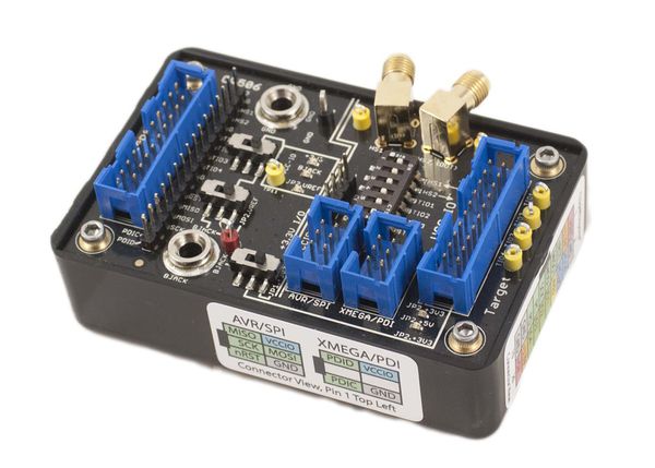
The CW506 is a simple but powerful breakout board for devices using NewAE Technology's 20-Pin Connector standard. Almost all of our target boards and capture hardware feature this connector, making the breakout board widely applicable to our product line.
The breakout board features a variety of voltage translators, test points, connectors, and switches that makes it simple to interface various test equipment and target devices together. This includes both connecting other lab equipment, along with connecting ChipWhisperer capture hardware to your own targets.
Connection Routing
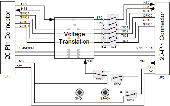
The following shows the routing of various connections on the breakout board:
Voltage Translation
The voltage translation is done with three different parts:
- SN74LVC1T45DBVT for high-speed clock lines (unidirectional, approx 200 Mbps max speed, 1.65V - 5.5V)
- PI4ULS5V201TAEX for GPIO1/2 (bidirectional, approx 20 Mbps max speed, 1.2V - 5.5V)
- GTL2003PW for GPIO2/3 + Others (bidirectional, 1.0V - 5.5V)
Note the clock translators limit lower operating voltage, if not using HS1 or HS2 you can safely use this board down to 1.2V. The maximum speed of the voltage translators varies with different output voltages, see datasheet for details.
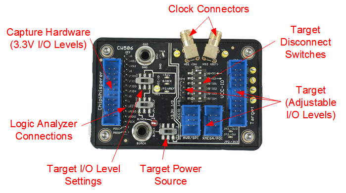
The VCCIO net on the board defines what logic level the target (i.e., the signals on the jumpers and headers on the right side of the board) section operates at. There is a vertical double-line on the breakout board, everything on the right side of the double-line operates at VCC-IO levels.
SW4 (Target Disconnect)
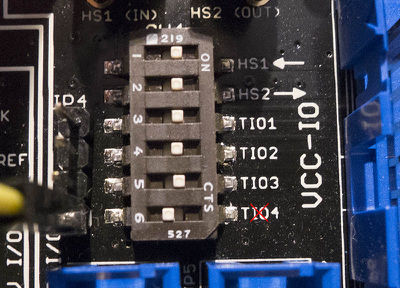
A DIP switch can be used to disconnect certain pins of the 20-pin header. The DIP switch has small text marked "ON", when the DIP switch is moved to this position the 20-pin connector is ENABLED.
The following shows an example where we've disconnected GPIO4 (the trigger) from our target device, and am feeding an external trigger in with the header (JP4) to the left of the DIP switch. This new trigger signal will be routed to the attached ChipWhisperer, and can be used instead of the trigger coming from the target device. Notice the DIP switch for TIO4 (GPIO4/IO4) is set to the LEFT, and the rest are set to the RIGHT (ON).
The following summarizes the connection for different SW4 settings. Note the 20-pin connector and the test-points to the right of that connector (marked TIO1, TIO2, TIO3, TIO4) are the only things disconnected.| 3.3V Logic | VCC-IO Logic | ||||||
|---|---|---|---|---|---|---|---|
| SW4 Setting | JP1 (Left 20-Pin) | JP3 | JP4 | JP5/JP6 | JP2 (Right 20-Pin) | TIO1-TIO4 Test Points | TP7/TP8, SMA Connectors |
| OFF | TIO1-TIO4 | ☑ | ☑ | ||||
| ON | TIO1-TIO4 | ☑ | ☑ | ☑ | ☑ | ||
| OFF | HS1-HS2 | ☑ | ☑ | ||||
| ON | HS1-HS2 | ☑ | ☑ | ☑ | |||
| ? | SPI/PDI/Other | ☑ | ☑ | ☑ | |||
VCC-IO Settings
The VCC-IO level defines what voltage the inputs/outputs on the RIGHT side operate at (the target side). The inputs/outputs on the LEFT side (the ChipWhisperer capture side) are always 3.3V.
The VCC-IO level can be set to one of:
- Fixed 3.3V.
- Based on voltage on VREF pin of JP2 (20-pin target connector).
- Based on external voltage reference.
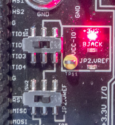
The current VCC-IO voltage is available on test point TP11 (just beside the 3 LEDs).
Normal Usage
Normally you would use either "JP2.VREF" or "+3V3". All NewAE target boards will provide a signal on JP2.VREF which indicates the correct translation voltage. If using a simple breakout or your own target board, you may just wish to force use of 3.3V IO voltages however.
These settings are configured with switch SW1 and SW2. In addition, three LEDs will confirm your setting. For example here the board is set to output 3.3V reference signals:
Using External VREF
The final setting allows you to use the banana jack (BJACK) or test point TP9 as the voltage reference. This allows usage of an external lab supply for setting the output signal level to any supported level.
If using the BJACK feature, be sure to check switch SW3 is set in the correct position. The BJACK can also be used to provide the 3.3V rail for the target device.
JP2.+3v3 Settings
The 20-pin target connector (JP2) has two power supplies: a +5.0V signal, and a +3.3V signal. Normally these signals would come from a power supply in the ChipWhisperer-Capture target board (on JP1).
However if using the breakout board stand-alone, these will not be present. Switch SW3 allows you to route an external power supply onto the +3.3V power supply pins of JP2, allowing you to power a target expecting this supply voltage. This can also be used to power a target that draws more current than the ChipWhisperer-Capture hardware can provide.
Note it's possible but not recommended to also use this feature to adjust the supply voltage of the target (i.e., experiment running the target at 2.5V or 5.0V). The 3.3V supply may power 3.3V-only logic on the target board.
Setting SW3 to the LEFT position will drive the 3.3V power supply on the target board from the banana jack connector, which also connect to test point TP9 (the large red test point).
XMEGA Programming & Voltage Levels
If you want to program an XMEGA target with the CW506 and CW-Lite, you'll have to place a resistor on your UFO Board. You must connect a 330 Ohm resistor between the GPIO3 and PDIC pin (you can use jumper cables instead of soldering or physically modifying your board).
To program the target set "Target IO3" to GPIO in "Scope Settings"-->"Target IOn pins". Next set GPIO3 to low from "Scope Settings"-->"Target IOn GPIO mode".
IMPORTANT: You must set GPIO3 to high after programming, otherwise the chip will remain in programming mode, and your code will not execute.
There is a known issue where GPIO3/4 do not reach VREF/VCCIO. Usually this does not cause problems, unless you are using a reference voltage above 3.3 volts. In some cases the high level voltage will be too close to its threshold to provide reliable performance. In this case a 330 Ohm pull up resistor between VREF and the affected pin should resolve the issue.
Use Cases
Probing Target Board Signals
Using Target Board Stand-Alone
Inserting External Equipment into Test Path
Schematic
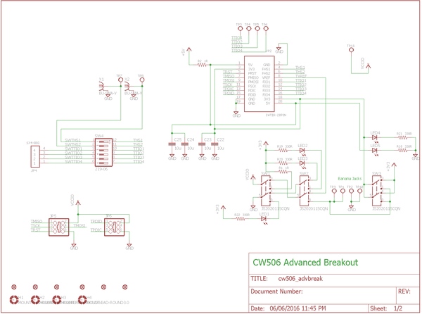
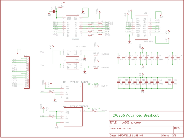
The schematic is available in two formats - PDF and schematic images. Click the images for full resolution.
