| As of August 2020 the site you are on (wiki.newae.com) is deprecated, and content is now at rtfm.newae.com. |
CW1200 ChipWhisperer-Pro
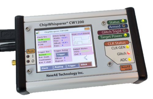
The CW1200 (ChipWhisperer Pro) is an upgraded version of the ChipWhisperer Lite capture hardware. The Pro includes an FPGA with much more space than the Lite, allowing many new features to be added, including a larger sample buffer, streaming-mode captures, additional trigger methods, and a touchscreen interface. These features make it a high-end device suitable for laboratory use.
Check out a sneak peek of the CW-Pro.
Contents
Power Supply
The ChipWhisperer Pro can only be powered through its 5 V jack. It cannot be powered through the USB port - internally, there are no connections to the USB port's 5 V rail. This limitation is primarily due to the high current draw of the Pro: while powering the touchscreen running and an external target, it would be easy to exceed the USB current limit, causing all sorts of issues.
To make this setup more flexible, the Pro ships with two power sources:
- A 5 V, 2.1 A power supply. This supply is suitable for a permanent bench setup.
- A USB-to-barrel jack cable. This solution is more portable: if you're travelling with a laptop, you can use a second USB port for power. A USB charger will also work here.
If you're using the USB power cable, it is recommended to use a separate power supply to power any external target boards.
Basic Usage
The basic features on the Pro are exactly the same as the ChipWhisperer Lite. This means that any scripts and tutorials made for the Lite will work on the Pro, too: the connectors and pinouts are exactly the same.
AVR Programmer
This section was recently updated for ChipWhisperer 5. The old version can be found here: https://wiki.newae.com/V4:CW1173_ChipWhisperer-Lite/AVR_Programmer.
The CW1173 and CW1200 have built-in support for programming either Atmel AVR or Atmel XMEGA device. This is designed to allow you to program our target boards (including the built-in XMEGA target).
Note this programmer is fairly simple, and does not provide all the features of a stand-alone programmer.
The AVR device programmer requires four connections to the target: RESET, MOSI, MISO, SCK. See #20-Pin_Connector for details of AVR programming pin connections.
Accessing the Programmer
First, setup the ChipWhisperer as usual:
import chipwhisperer as cw
scope = cw.scope()
target = cw.target(scope)
Next, the AVR programmer can be accessed through the cw.programmers.AVRProgrammer object:
prog = cw.programmers.AVRProgrammer
Programming the Flash
Note to use the AVR programmer you may require a valid clock source for the AVR. It is suggested to use the default ChipWhisperer setup, which will generate a 7.37MHz clock:
scope.default_setup()
Note that NewAE's Notduino targets have the transmit and receive pins swapped compared to the usual targets. If you're using one of these targets, swap them using the API:
scope.io.tio1 = "serial_tx"
scope.io.tio2 = "serial_rx"
Next, try programming the device by calling cw.program_target():
cw.program_target(scope, prog, "<path to hex file")
The default SPI data rate for the programmer is too fast for devices which are running slower than 2 MHz. If programming a device with a clock source slower than 2 MHz, you will need to enable the "Slow Clock Mode". In "Slow Clock Mode" the entire SAM3U and FPGA clock is changed from 96 MHz to 12 MHz. Note the default fuse bytes for a virgin ATMega328P result in a 1 MHz clock, so you will need to use "slow clock mode" to program the correct fuse bytes, after which point you will not need to use "slow clock mode".
To enable slow clock mode, call program_target with an additional slow_clock = True parameter:
cw.program_target(scope, prog, "<path to hex file", slow_clock=True)
noteThe 'slow clock mode' is used to provide a slower SPI clock than would otherwise be possible. When switching into 'slow clock mode' it will cause all DCM blocks in the FPGA to become unlocked. You will need to reset the DCM blocks, or simply call
default_setup()again (this will reset the serial pins, so you'll have to swap them again if you're using a Notduino target).
Programming the Fuses
By default the AVR programmer allows you to modify the LOW fuse byte only, as this byte controls the clock source selection. To change the value of the fuse byte, you'll need to manually setup the programmer:
avr_programmer = prog(slow_clock=False) #call with slow_clock = True to enable the slow clock
avr_programmer.scope = scope
avr_programmer.open()
avr_programmer.find()
Once that's accomplished, the readFuse() and writeFuse() methods can be used to read and write the fuse bits, respectively:
fuse_vals = avr_programmer.readFuse(<value>)
avr_programmer.writeFuse(<value>, <lfuse>)
with <value> corresponding to one of the following: "low", "high", or "extended".
See an Online Fuse Calculator to better understand what the values mean.
tip
- If programming a virgin ATMega328P device, the default low-fuse value of
62results in the internal 8 MHz oscillator being divided down to 1 MHz. Any external clock is ignored.The low fuse byte must be changed to
D0to use the external clock provided by the ChipWhisperer toolchain.
Troubleshooting
If you run into issues when programming the AVR, try the following troubleshooting methods:
- Ensure the ChipWhisperer is outputting a clock if the target requires one.
- Ensure you have the serial pins the right way around
- Ensure the fuse bits are set correctly.
XMEGA Programmer
This section has been recently updated for ChipWhisperer 5. The previous version can be found here: https://wiki.newae.com/V4:CW1173_ChipWhisperer-Lite/XMEGA_Programmer
The XMEGA device programmer requires only two connections to the target: clock (PDIC) and data (PDID). The PDIC line is usually shared with the RESET pin, and the PDID pin is a specific pin on the XMEGA device. See #20-Pin_Connector for details of XMEGA programming pin connections. Once you have the scope setup, the programmer can be accessed through cw.programmers.XMEGAProgrammer:
prog = cw.programmers.XMEGAProgrammer
cw.program_target(scope, prog, "<path to fw hex file>")
Using Glitch Port
This section has been recently updated for ChipWhisperer 5. The previous version can be found here: https://wiki.newae.com/V4:CW1173_ChipWhisperer-Lite/XMEGA_Programmer
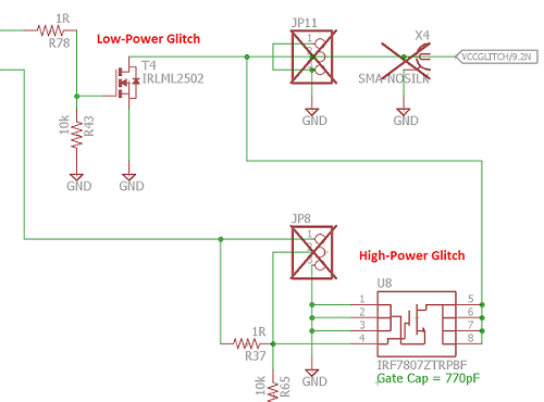
The "GLITCH" port is used for voltage glitching. It's connected to two MOSFET elements, as the following figure shows:
The CW1173 glitch output can be commanded to turn on either of those MOSFETs via scope.io.glitch_hp and scope.io.glitch_lp fields:
scope.io.glitch_hp = True #enable high power glitch
scope.io.glitch_hp = False #disable high power glitch

scope.io.glitch_lp = True #enable low power glitch
scope.io.glitch_lp = False #disable low power glitch
Be careful using this feature, as you don't want to short the MOSFETs for too long. It's also possible to damage the ChipWhisperer-Lite by burning these MOSFETs up if used incorrectly. See tutorial Fault_2 (https://chipwhisperer.readthedocs.io/en/latest/tutorials/fault_2-openadc-cwlitearm.html#tutorial-fault-2-openadc-cwlitearm) for more information.
Using Measure Port
The "MEASURE" port is the input to the low-noise amplifier and ADC.
== Using Measure Port == The "MEASURE" port is the input to the low-noise amplifier and ADC.
20-Pin Connector
The pinout is as follows:
| Number | Name | Dir | Description |
|---|---|---|---|
| 1 | +VUSB (5V) | O | Not Connected on ChipWhisperer-Lite. |
| 2 | GND | O | System GND. |
| 3 | +3.3V | O | +3.3V to Target Device, can be turned off, 200mA available. |
| 4 | FPGA-HS1 | I/O | High Speed Input (normally clock in). |
| 5 | PROG-RESET | I/O | Target RESET Pin (AVR Programmer). |
| 6 | FPGA-HS2 | I/O | High Speed Output (normally clock or glitch out). |
| 7 | PROG-MISO | I/O | SPI input: MISO (for SPI + AVR Programmer). |
| 8 | VTarget | I | Drive this pin with desired I/O voltage in range 1.5V-5V. |
| 9 | PROG-MOSI | I/O | SPI output: MOSI (for SPI + AVR Programmer). |
| 10 | FPGA-TARG1 | I/O | TargetIO Pin 1 - Usually UART TX or RX. |
| 11 | PROG-SCK | I/O | SPI output: SCK (for SPI + AVR Programmer). |
| 12 | FPGA-TARG2 | I/O | TargetIO Pin 2 - Usually UART RX or TX. |
| 13 | PROG-PDIC | I/O | PDI Programming Clock (XMEGA Programmer), or CS pin (SPI). |
| 14 | FPGA-TARG3 | I/O | TargetIO Pin 3 - Usually bidirectional IO for smartcard. |
| 15 | PROG-PDID | I/O | PDI Programming Data (XMEGA Programmer). |
| 16 | FPGA-TARG4 | I/O | TargetIO Pin 4 - Usually trigger input. |
| 17 | GND | O | |
| 18 | +3.3V | O | |
| 19 | GND | O | |
| 20 | +VUSB (5V) | O | Not Connected on ChipWhisperer-Lite. |
== 20-Pin Connector == The pinout is as follows:
| Number | Name | Dir | Description |
|---|---|---|---|
| 1 | +VUSB (5V) | O | Not Connected on ChipWhisperer-Lite. |
| 2 | GND | O | System GND. |
| 3 | +3.3V | O | +3.3V to Target Device, can be turned off, 200mA available. |
| 4 | FPGA-HS1 | I/O | High Speed Input (normally clock in). |
| 5 | PROG-RESET | I/O | Target RESET Pin (AVR Programmer). |
| 6 | FPGA-HS2 | I/O | High Speed Output (normally clock or glitch out). |
| 7 | PROG-MISO | I/O | SPI input: MISO (for SPI + AVR Programmer). |
| 8 | VTarget | I | Drive this pin with desired I/O voltage in range 1.5V-5V. |
| 9 | PROG-MOSI | I/O | SPI output: MOSI (for SPI + AVR Programmer). |
| 10 | FPGA-TARG1 | I/O | TargetIO Pin 1 - Usually UART TX or RX. |
| 11 | PROG-SCK | I/O | SPI output: SCK (for SPI + AVR Programmer). |
| 12 | FPGA-TARG2 | I/O | TargetIO Pin 2 - Usually UART RX or TX. |
| 13 | PROG-PDIC | I/O | PDI Programming Clock (XMEGA Programmer), or CS pin (SPI). |
| 14 | FPGA-TARG3 | I/O | TargetIO Pin 3 - Usually bidirectional IO for smartcard. |
| 15 | PROG-PDID | I/O | PDI Programming Data (XMEGA Programmer). |
| 16 | FPGA-TARG4 | I/O | TargetIO Pin 4 - Usually trigger input. |
| 17 | GND | O | |
| 18 | +3.3V | O | |
| 19 | GND | O | |
| 20 | +VUSB (5V) | O | Not Connected on ChipWhisperer-Lite. |
Upgrading SAM3U Firmware
This section has been recently updated for ChipWhisperer 5. The previous version can be found here: https://wiki.newae.com/V4:CW1173_ChipWhisperer-Lite/Upgrading_SAM3U_Firmware
When talking about the ChipWhisperer's firmware, there is really two parts to this:
- The FPGA Bitstream file.
- The SAM3U USB interface chip firmware.
The FPGA bitstream alone is what is normally configured by the ChipWhisperer-Capture software. This bitstream is always the most up-to-date, since it's automatically reloaded by the computer every time you power cycle the ChipWhisperer-Capture. The SAM3U firmware however is not automatically updated, but it tends to change less frequently.
Checking Firmware Version
The firmware version is printed at start-up. You will see a line that looks like this indicating the version of the SAM3U Firmware:
Found CW-Lite, Serial Number = 442031204630xxxxxxxxxxx
SAM3U Firmware version = 0.11 b0
Programmed FPGA
If your firmware version is outdated, a warning will be printed. You can also see the firmware version in the Config CW Firmware dialog:
Note the main version is 0.11 in this example. The "b0" indicates a "build" number. Typically this will be "build 0", but special versions will use a different build number to indicate a variant of a regular version.
Upgrading Firmware
See https://chipwhisperer.readthedocs.io/en/latest/api.html#firmware-update for instructions on how to update the SAM3U firmware.
Linux usbserial module Workaround
There is an issue in some versions of Linux, where the SAM3U is not assigned a serial port when it enters bootloader mode. Here are some steps to resolve this issue (Note. this is not a permanent fix, you must go through these steps each time you put your ChipWhisperer into bootloader mode.). These steps assume you've already put ChipWhisperer into bootloader mode.
- Unplug your ChipWhisperer (Leave unplugged until instructed otherwise)
- Reboot your computer
- Once logged in again, open a terminal session
- Run this command:
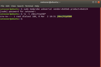
sudo modprobe usbserial vendor=0x3eb product=0x6124 - Plug your ChipWhisperer back in
- Check that a serial port is now open using:
ls -l /dev/ttyUSB*
You should now be able to program the bootloader from ChipWhisperer Capture through the port you created
Manual Update
If the above instructions fail, there is no big problem. The SAM3U chip contains a hardware-resident bootloader. You may need to follow instructions on the Manual SAM3U Firmware Update page (including using BOSSA) if you are unable to use the automatic system that is part of ChipWhisperer-Capture.
Advanced Features
Streaming Mode
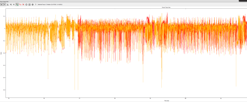
The ChipWhisperer Pro has a streaming mode that allows extremely long captures as long as relatively low sampling rates are used. For example, this plot shows an exerpt from two traces with nearly 1 million samples:
This capture mode is useful for many types of attacks, including:
- Full captures of slow software AES libraries
- Power analysis on ECC
- Context switches on embedded operating systems
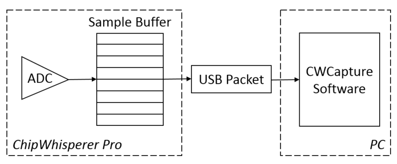
While streaming, the ChipWhisperer hardware sends ADC data back to the capture software while recording more samples (instead of waiting until the end of the capture). During this process, the ADC samples are sent back to the computer in packets of approximately 3000 samples at a time. As a block diagram, this looks like:
The main danger in streaming mode is that the FPGA's sample buffer can overflow if the PC doesn't request these packets quickly enough. In practice, the maximum transfer rate is around 10 Msamples/s, so the maximum ADC frequency is approximately 10 MHz in streaming mode. Trying to stream above this rate will usually cause data to be lost: the FPGA overwrites samples after the buffer is full, so it's impossible to recover these samples after overrunning the buffer.
On the software end, there are two things to watch for:
- Long captures from streaming mode (millions of points) may take several seconds to record. When working with these long captures, make sure the software's timeouts are long enough.
- Extremely long captures take a lot of memory. 64-bit Python is recommended if you plan on capturing many traces with millions of samples - you can hit the memory limit on 32-bit Python pretty quickly.
== Streaming Mode == The ChipWhisperer Pro has a streaming mode that allows extremely long captures as long as relatively low sampling rates are used. For example, this plot shows an exerpt from two traces with nearly 1 million samples:
This capture mode is useful for many types of attacks, including:
- Full captures of slow software AES libraries
- Power analysis on ECC
- Context switches on embedded operating systems
While streaming, the ChipWhisperer hardware sends ADC data back to the capture software while recording more samples (instead of waiting until the end of the capture). During this process, the ADC samples are sent back to the computer in packets of approximately 3000 samples at a time. As a block diagram, this looks like:
The main danger in streaming mode is that the FPGA's sample buffer can overflow if the PC doesn't request these packets quickly enough. In practice, the maximum transfer rate is around 10 Msamples/s, so the maximum ADC frequency is approximately 10 MHz in streaming mode. Trying to stream above this rate will usually cause data to be lost: the FPGA overwrites samples after the buffer is full, so it's impossible to recover these samples after overrunning the buffer.
On the software end, there are two things to watch for:
- Long captures from streaming mode (millions of points) may take several seconds to record. When working with these long captures, make sure the software's timeouts are long enough.
- Extremely long captures take a lot of memory. 64-bit Python is recommended if you plan on capturing many traces with millions of samples - you can hit the memory limit on 32-bit Python pretty quickly.
Trigger Module
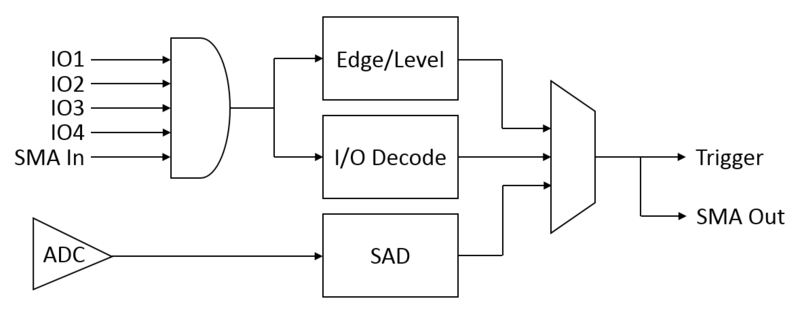
Unlike the ChipWhisperer-Lite, the Pro has three different trigger modes to help capture traces when it's difficult to get a concrete trigger signal. A block diagram of the trigger module is:
The first two trigger modes use a combination of the trigger inputs - the four GPIO inputs and the auxiliary SMA input. In the Capture software, these five inputs can be enabled independently and combined in three methods (AND, OR, and NAND). This combined trigger signal is the input for the edge/level and I/O decode detectors. The last trigger mode looks directly at the power trace and does not use these trigger inputs.
Edge/Level
The edge/level detector can trigger on four different events:
- Trigger input is low (0)
- Trigger input is high (1)
- Trigger input had a rising edge (0 -> 1)
- Trigger input had a falling edge (1 -> 0)
This mode is suitable when the target is using one of the GPIO pins as a trigger signal - if you have control over the target's source code, let it output a rising edge when the encryption or other operation begins.
I/O Decoder
The I/O decoder examines the trigger signal, assumes that it is either UART or SPI traffic, and outputs a trigger signal when it detects a certain pattern on the line. In the capture software, the settings for this decoder are:
- Decode Type: Which type of traffic is being captured in the trigger signal? Might be USART or SPI data.
- Trigger Data: Which data are we searching for? This setting should be a list of bytes to be detected in order. For example,
['r', '0']would detect the string "r0", and[0x07]would detect a bell character. - Baud: What baud rate does this line use? This needs to be set manually.
When using this trigger mode, target IO1/IO2 are probably the best inputs to use: these are normally the serial TX and RX lines. It's possible to enable either one of these to trigger on sending or receiving data, respectively.
Sum of Absolute Differences (SAD)
Some targets don't have nice trigger signals to detect. Sad!
The Sum of Absolute Differences module has two 128 sample buffers. The FPGA stores the ADC's 128 most recent samples in one buffer and a fixed pattern in the other. Then, after every sample, it calculates

If this sum is below a fixed threshold, the output trigger signal will be set. This trigger module allows the ChipWhisperer to detect a specific pattern (for instance, an encryption operation) in a power trace without any other data.
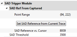
The settings for the SAD module are:
- Point Range: The samples in the current trace to be used for the SAD module's fixed values. This range is forced to have a width of 128.
- Set SAD Reference from Current Trace: Sets the fixed 128 samples to the current selection.
- SAD Reference vs. Cursor: Shows the current output of the SAD calculation. Useful for setting the threshold - it's easy to capture a number of traces and check what typical values are for this SAD output.
- SAD Threshold: The trigger point for the SAD module. A value of 0 indicates a perfect match. If this threshold is too low, noise will stop the trigger from appearing; if it's too high, the scope will trigger at random offsets.
Note that this SAD module does not play well with downsampling: the inputs to the SAD buffer are not downsampled. This means that downsampled traces cannot be used as a reference. If you want to use this trigger type, set up your SAD trigger with downsampling turned off first.
== Trigger Module == Unlike the ChipWhisperer-Lite, the Pro has three different trigger modes to help capture traces when it's difficult to get a concrete trigger signal. A block diagram of the trigger module is:
The first two trigger modes use a combination of the trigger inputs - the four GPIO inputs and the auxiliary SMA input. In the Capture software, these five inputs can be enabled independently and combined in three methods (AND, OR, and NAND). This combined trigger signal is the input for the edge/level and I/O decode detectors. The last trigger mode looks directly at the power trace and does not use these trigger inputs.
Edge/Level
The edge/level detector can trigger on four different events:
- Trigger input is low (0)
- Trigger input is high (1)
- Trigger input had a rising edge (0 -> 1)
- Trigger input had a falling edge (1 -> 0)
This mode is suitable when the target is using one of the GPIO pins as a trigger signal - if you have control over the target's source code, let it output a rising edge when the encryption or other operation begins.
I/O Decoder
The I/O decoder examines the trigger signal, assumes that it is either UART or SPI traffic, and outputs a trigger signal when it detects a certain pattern on the line. In the capture software, the settings for this decoder are:
- Decode Type: Which type of traffic is being captured in the trigger signal? Might be USART or SPI data.
- Trigger Data: Which data are we searching for? This setting should be a list of bytes to be detected in order. For example,
['r', '0']would detect the string "r0", and[0x07]would detect a bell character. - Baud: What baud rate does this line use? This needs to be set manually.
When using this trigger mode, target IO1/IO2 are probably the best inputs to use: these are normally the serial TX and RX lines. It's possible to enable either one of these to trigger on sending or receiving data, respectively.
Sum of Absolute Differences (SAD)
Some targets don't have nice trigger signals to detect. Sad!
The Sum of Absolute Differences module has two 128 sample buffers. The FPGA stores the ADC's 128 most recent samples in one buffer and a fixed pattern in the other. Then, after every sample, it calculates

If this sum is below a fixed threshold, the output trigger signal will be set. This trigger module allows the ChipWhisperer to detect a specific pattern (for instance, an encryption operation) in a power trace without any other data.
The settings for the SAD module are:
- Point Range: The samples in the current trace to be used for the SAD module's fixed values. This range is forced to have a width of 128.
- Set SAD Reference from Current Trace: Sets the fixed 128 samples to the current selection.
- SAD Reference vs. Cursor: Shows the current output of the SAD calculation. Useful for setting the threshold - it's easy to capture a number of traces and check what typical values are for this SAD output.
- SAD Threshold: The trigger point for the SAD module. A value of 0 indicates a perfect match. If this threshold is too low, noise will stop the trigger from appearing; if it's too high, the scope will trigger at random offsets.
Note that this SAD module does not play well with downsampling: the inputs to the SAD buffer are not downsampled. This means that downsampled traces cannot be used as a reference. If you want to use this trigger type, set up your SAD trigger with downsampling turned off first.
SMA I/O
The Pro has an extra SMA connector intended to be used for additional trigger logic. It can be used either as a trigger input or output.
Input: The Aux SMA trigger input can be used in the exact same manner as the other trigger inputs: the digital level is combined with the other active triggers (through an AND or OR gate) and this is used as the trigger signal. This is helpful for using other creative trigger signals. For example, if you have a custom target board, you could connect an FPGA output as an additional trigger signal. Alternatively, you could use a high-end oscilloscope's pattern detection as a trigger input.
Output: When the trigger module produces a trigger signal, the ChipWhisperer can reproduce this signal on the Aux SMA. This allows an external oscilloscope to be used to capture traces alongside the ChipWhisperer.
== SMA I/O == The Pro has an extra SMA connector intended to be used for additional trigger logic. It can be used either as a trigger input or output.
Input: The Aux SMA trigger input can be used in the exact same manner as the other trigger inputs: the digital level is combined with the other active triggers (through an AND or OR gate) and this is used as the trigger signal. This is helpful for using other creative trigger signals. For example, if you have a custom target board, you could connect an FPGA output as an additional trigger signal. Alternatively, you could use a high-end oscilloscope's pattern detection as a trigger input.
Output: When the trigger module produces a trigger signal, the ChipWhisperer can reproduce this signal on the Aux SMA. This allows an external oscilloscope to be used to capture traces alongside the ChipWhisperer.
Touchscreen
The touchscreen on the ChipWhisperer Pro shows various details about its status and current settings.
Screen 1: Clock
The clock screen shows the status of the CLKGEN and ADC clocks along with the frequency counter.
TODO: picture
- CLKGEN: Current frequency of CLKGEN clock in kHz
- Source: Input to CLKGEN DCM. Could be system clock or EXTCLK
- DCM: Lock status of CLKGEN DCM
- Reset DCM: Reset the CLKGEN output. Useful if clock has locked at the wrong frequency
- ADC Clock: Current ADC sampling rate in kHz
- Source: Input to ADC DCM. Could be related to CLKGEN or EXTCLK
- DCM: Lock status of ADC DCM
- Reset DCM: Reset the ADC clock output
- Frequency Counter: Current frequency measured by the frequency counter
- Source: Input to frequency counter. Could be either EXTCLK or CLKGEN
Screen 2: Routing
The routing screen shows the status of the various I/O pins.
TODO: picture
- Aux Output: Status of the aux SMA connections. Could be used as trigger input/output, glitch output, and/or clock output
- IO Pins: Status of each of the IO pins on the 20 pin connector. Possible values depend on pin
- Target Power State: Status of the 3.3 V output. Can be toggled here to reset target
- Target HS IO-Out: Signal connected to high-speed output (HS2). Could be CLKGEN, glitch module, or disabled
Screen 3: Trigger
The trigger screen shows the current settings for the trigger module and the ADC capture settings.
TODO: picture
- Trigger Pins: Whether each trigger input is enabled. Active inputs are highlighted
- Mode: Trigger combination method. Could be AND, OR, or NAND
- Trigger Source: The trigger type in use. Active trigger module is highlighted
- State: The current output level of the trigger module
- Trigger Mode: The ADC trigger type. Active mode is highlighted
- Samples:
- Delay: Current ADC offset. This is the number of samples to wait after trigger before recording begins
- Pre: Number of pre-trigger samples to be saved
- Time: Delay, but converted into a time
- Total: Number of samples to be recorded in total
- ADC gain:
- Mode: Amplification type. Either low or high
- Setting: Low noise amplifier gain level
Screen 4: Glitch
The glitch screen shows the current settings for the glitch module.
TODO: picture
- Clock Src: Input to the glitch module's clock. Active clock is highlighted
- DCM: Lock status of the glitch module's DCM
- Glitch Setup:
- Width: Duty cycle of glitch pulse, as a fraction of one period
- Fine: Adjustment on width
- Offset: Distance between clock rising edge and glitch pulse rising edge, as a fraction of one period
- Fine: Adjustment on offset
- View: Schematic of glitch clock. Shows regular clock above (blue) and glitch module output below (black)
- Trigger Src: Input for glitch module. Active source is highlighted
- Trigger Setup:
- Trigger: Cause a manual trigger. Has no effect unless trigger source is set to Manual
- Offset: Number of cycles to wait before starting glitch pulses
- Repeat: Number of consecutive pulses to generate
- Output Status
- VCC: Status of glitching MOSFETs. Shows warning sign if VCC glitching is enabled
- Cnt: Total number of glitch pulses generated
= Touchscreen = The touchscreen on the ChipWhisperer Pro shows various details about its status and current settings.
Screen 1: Clock
The clock screen shows the status of the CLKGEN and ADC clocks along with the frequency counter.
TODO: picture
- CLKGEN: Current frequency of CLKGEN clock in kHz
- Source: Input to CLKGEN DCM. Could be system clock or EXTCLK
- DCM: Lock status of CLKGEN DCM
- Reset DCM: Reset the CLKGEN output. Useful if clock has locked at the wrong frequency
- ADC Clock: Current ADC sampling rate in kHz
- Source: Input to ADC DCM. Could be related to CLKGEN or EXTCLK
- DCM: Lock status of ADC DCM
- Reset DCM: Reset the ADC clock output
- Frequency Counter: Current frequency measured by the frequency counter
- Source: Input to frequency counter. Could be either EXTCLK or CLKGEN
Screen 2: Routing
The routing screen shows the status of the various I/O pins.
TODO: picture
- Aux Output: Status of the aux SMA connections. Could be used as trigger input/output, glitch output, and/or clock output
- IO Pins: Status of each of the IO pins on the 20 pin connector. Possible values depend on pin
- Target Power State: Status of the 3.3 V output. Can be toggled here to reset target
- Target HS IO-Out: Signal connected to high-speed output (HS2). Could be CLKGEN, glitch module, or disabled
Screen 3: Trigger
The trigger screen shows the current settings for the trigger module and the ADC capture settings.
TODO: picture
- Trigger Pins: Whether each trigger input is enabled. Active inputs are highlighted
- Mode: Trigger combination method. Could be AND, OR, or NAND
- Trigger Source: The trigger type in use. Active trigger module is highlighted
- State: The current output level of the trigger module
- Trigger Mode: The ADC trigger type. Active mode is highlighted
- Samples:
- Delay: Current ADC offset. This is the number of samples to wait after trigger before recording begins
- Pre: Number of pre-trigger samples to be saved
- Time: Delay, but converted into a time
- Total: Number of samples to be recorded in total
- ADC gain:
- Mode: Amplification type. Either low or high
- Setting: Low noise amplifier gain level
Screen 4: Glitch
The glitch screen shows the current settings for the glitch module.
TODO: picture
- Clock Src: Input to the glitch module's clock. Active clock is highlighted
- DCM: Lock status of the glitch module's DCM
- Glitch Setup:
- Width: Duty cycle of glitch pulse, as a fraction of one period
- Fine: Adjustment on width
- Offset: Distance between clock rising edge and glitch pulse rising edge, as a fraction of one period
- Fine: Adjustment on offset
- View: Schematic of glitch clock. Shows regular clock above (blue) and glitch module output below (black)
- Trigger Src: Input for glitch module. Active source is highlighted
- Trigger Setup:
- Trigger: Cause a manual trigger. Has no effect unless trigger source is set to Manual
- Offset: Number of cycles to wait before starting glitch pulses
- Repeat: Number of consecutive pulses to generate
- Output Status
- VCC: Status of glitching MOSFETs. Shows warning sign if VCC glitching is enabled
- Cnt: Total number of glitch pulses generated
