| As of August 2020 the site you are on (wiki.newae.com) is deprecated, and content is now at rtfm.newae.com. |
Difference between revisions of "CW308 UFO Target"
(→Usage Example: Stand-Alone) |
|||
| Line 796: | Line 796: | ||
{{Template:Hardware}} | {{Template:Hardware}} | ||
| + | |||
| + | |||
| + | [[Category:Hardware]] | ||
| + | [[Category:Targets]] | ||
| + | [[Category:CW308 Targets]] | ||
Revision as of 09:27, 25 March 2017
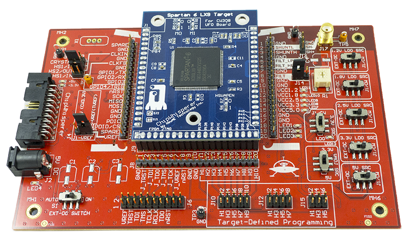
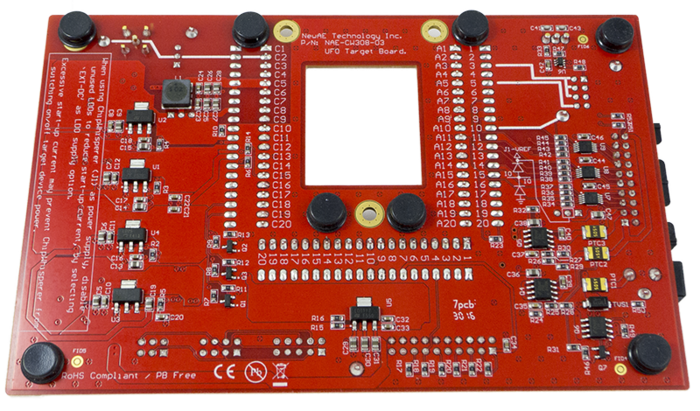
The CW308 UFO Board is a handy main-board for attacking all sorts of embedded targets. Released in 2016, it forms the basis for most of our upcoming target boards. It can be used stand-alone (with an oscilloscope) or with the ChipWhisperer-Capture hardware.
Contents
Supported Targets
Details of the targets are held on their own wiki page. Some targets are available premade, but all have gerber files in the GIT repo so you can build them yourself.
- CW308T-GENERIC (Protoboard)
- CW308T-AVR (Atmel AVR, 8-bit)
- CW308T-XMEGA (Atmel XMEGA, 8-bit)
- CW308T-87C51 (Intel 87C51RB, 8-bit)
- CW308T-ATSAMR21 (Atmel SAMR21 with 802.15.4 radio, 32-bit ARM Cortex M0)
- CW308T-MEGARF (Atmel MegaRF2564RFR2, 8-bit AVR)
- CW308T-MSP430FR5 (TI MSP430FR5xxx, 16-bit)
- CW308T-S6LX9 (Xilinx Spartan 6 LX9 in TQFP, FPGA)
If you need to support a new target, it's generally very simple to build a custom board.
Victim Board Connectors
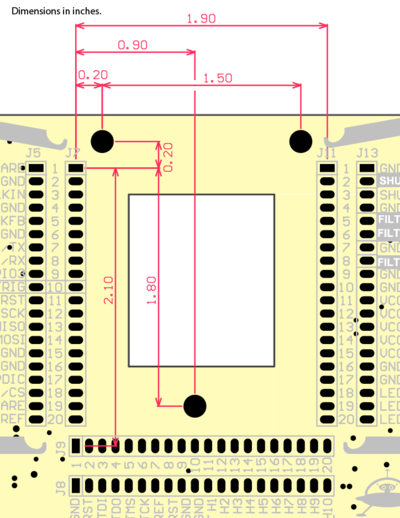
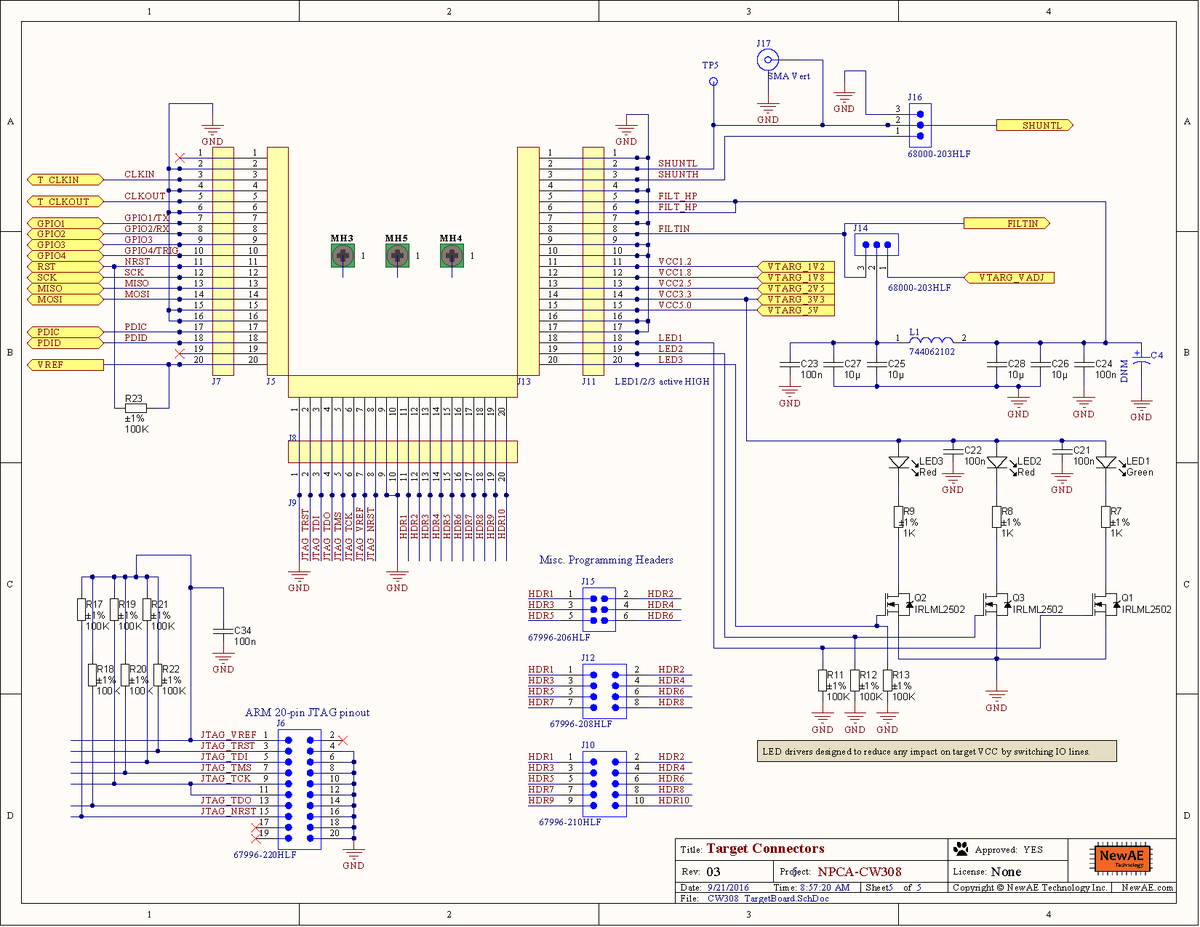
The "victim board" fits into three 20-pin female headers. They provide both electrical and mechanical connections for the board. There is optional mounting holes which can be used if additional mechanical support is required (especially if you need a locked-down victim for use with an EM probe).
The following shows the dimensions of the main connector:
Note the middle mounting hole is slightly offset to one direction! This was done to keep the mounting hole on a 100-mil grid spacing.
| J7 (West, A) | Function | Direction | Notes |
|---|---|---|---|
| 1 | Spare | Not connected to main-board, can be used as spare I/O pin breakout. | |
| 2 | GND | ||
| 3 | CLK-IN | CW308 --> Victim | Clock to victim. |
| 4 | GND | ||
| 5 | CLKOUT | CW308 <-- Victim | |
| 6 | GND | ||
| 7 | GPIO1 | ||
| 8 | GPIO2 | ||
| 9 | GPIO3 | ||
| 10 | GPIO4 | ||
| 11 | nRST | CW308 --> Victim | 100k pull-up to VREF. |
| 12 | SCK | ||
| 13 | MISO | ||
| 14 | MOSI | ||
| 15 | GND | ||
| 16 | GND | ||
| 17 | PDIC | ||
| 18 | PDID/CS | ||
| 19 | Spare | ||
| 20 | VREF | CW308 <-- Victim | Reference voltage for I/O. MUST be set to VCC-IO voltage (3.3V, etc) or I/O lines may not work. |
| J9 (South, B) | Function | Direction | Notes |
|---|---|---|---|
| 1 | GND | ||
| 2 | JTAG_TRST | Connects to 20-pin ARM JTAG header. | |
| 3 | JTAG_TDI | Connects to 20-pin ARM JTAG header. | |
| 4 | JTAG_TDO | Connects to 20-pin ARM JTAG header. | |
| 5 | JTAG_TMS | Connects to 20-pin ARM JTAG header. | |
| 6 | JTAG_TCK | Connects to 20-pin ARM JTAG header. | |
| 7 | JTAG_VREF | Connects to 20-pin ARM JTAG header. All JTAG_ pins have 100k pull-up to this pin. Must set to appropriate value. | |
| 8 | JTAG_nRST | Connects to 20-pin ARM JTAG header. | |
| 9 | GND | ||
| 10 | GND | ||
| 11 | HDR1 | J10, J12, J15: Pin 1 | |
| 12 | HDR2 | J10, J12, J15: Pin 2 | |
| 13 | HDR3 | J10, J12, J15: Pin 3 | |
| 14 | HDR4 | J10, J12, J15: Pin 4 | |
| 15 | HDR5 | J10, J12, J15: Pin 5 | |
| 16 | HDR6 | J10, J12, J15: Pin 6 | |
| 17 | HDR7 | J10, J12: Pin 7 | |
| 18 | HDR8 | J10, J12: Pin 8 | |
| 19 | HDR9 | J10: Pin 9 | |
| 20 | HDR10 | J10: Pin 10 |
| J11 (East, C) | Function | Direction | Notes |
|---|---|---|---|
| 1 | GND | ||
| 2 | SHUNTL | Low-Side Shunt Connection (connects to SMA) | |
| 3 | SHUNTH | High-Side Shunt Connection (power input side) | |
| 4 | GND | ||
| 5 | FILT_HP | CW308 --> Victim | High-Power filter output (same as FILT_LP on this hardware) |
| 6 | FILT_LP | CW308 --> Victim | Low-Power filter output (same as FILT_HP on this hardware) |
| 7 | GND | ||
| 8 | FILTIN | CW308 <-- Victim | Input to power supply filter. |
| 9 | GND | ||
| 10 | GND | ||
| 11 | 1.2V | CW308 --> Victim | 1.2V LDO Regulator output |
| 12 | 1.8V | CW308 --> Victim | 1.8V LDO Regulator output |
| 13 | 2.5V | CW308 --> Victim | 2.5V LDO Regulator output |
| 14 | 3.3V | CW308 --> Victim | 3.3V LDO Regulator output OR 3.3V from 20-pin connector |
| 15 | 5.0V | CW308 --> Victim | 5.0V from either DC-Power jack or 20-pin connector |
| 16 | GND | ||
| 17 | GND | ||
| 18 | LED1 | CW308 <-- Victim | Active-high buffered LED driver. 100k pull-down. |
| 19 | LED2 | CW308 <-- Victim | Active-high buffered LED driver. 100k pull-down. |
| 20 | LED3 | CW308 <-- Victim | Active-high buffered LED driver. 100k pull-down. |
Removing / Replacing Victim Boards
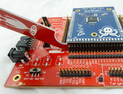
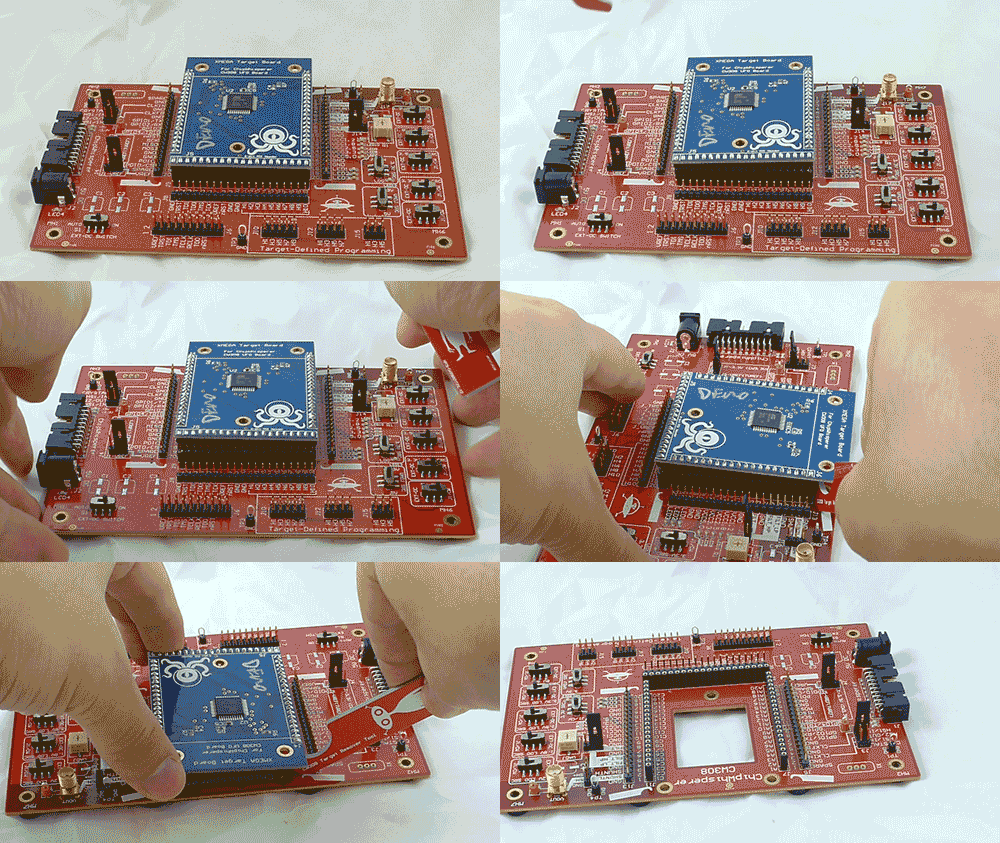
The target board is removed and replaced using the removal tool. This helps avoid bending pins:
The following shows the removal process:
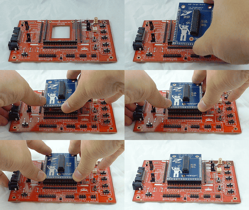
Adding a board involves carefully aligning the board and pushing down:
The alignment should be carefully checked if resistance is found. You may need to adjust how the board is aligned, as you should be able to press down with minimal force.
The CW308 should be turned off when swapping victim boards.
I/O Connections
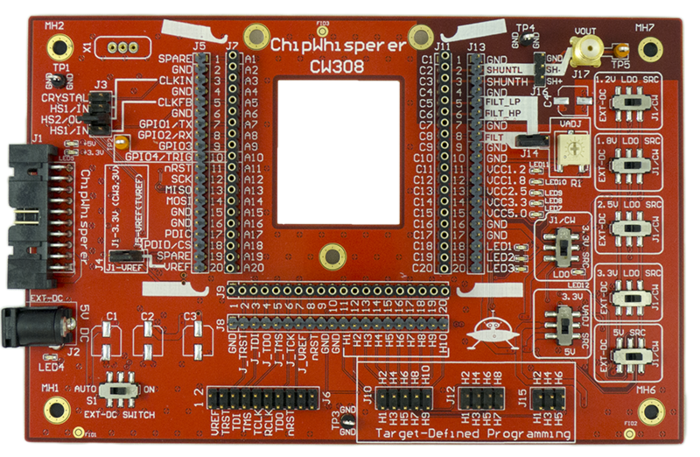
There are two main I/O connection points: the pin headers which duplicate the target board connections, and the 20-pin ChipWhisperer header.
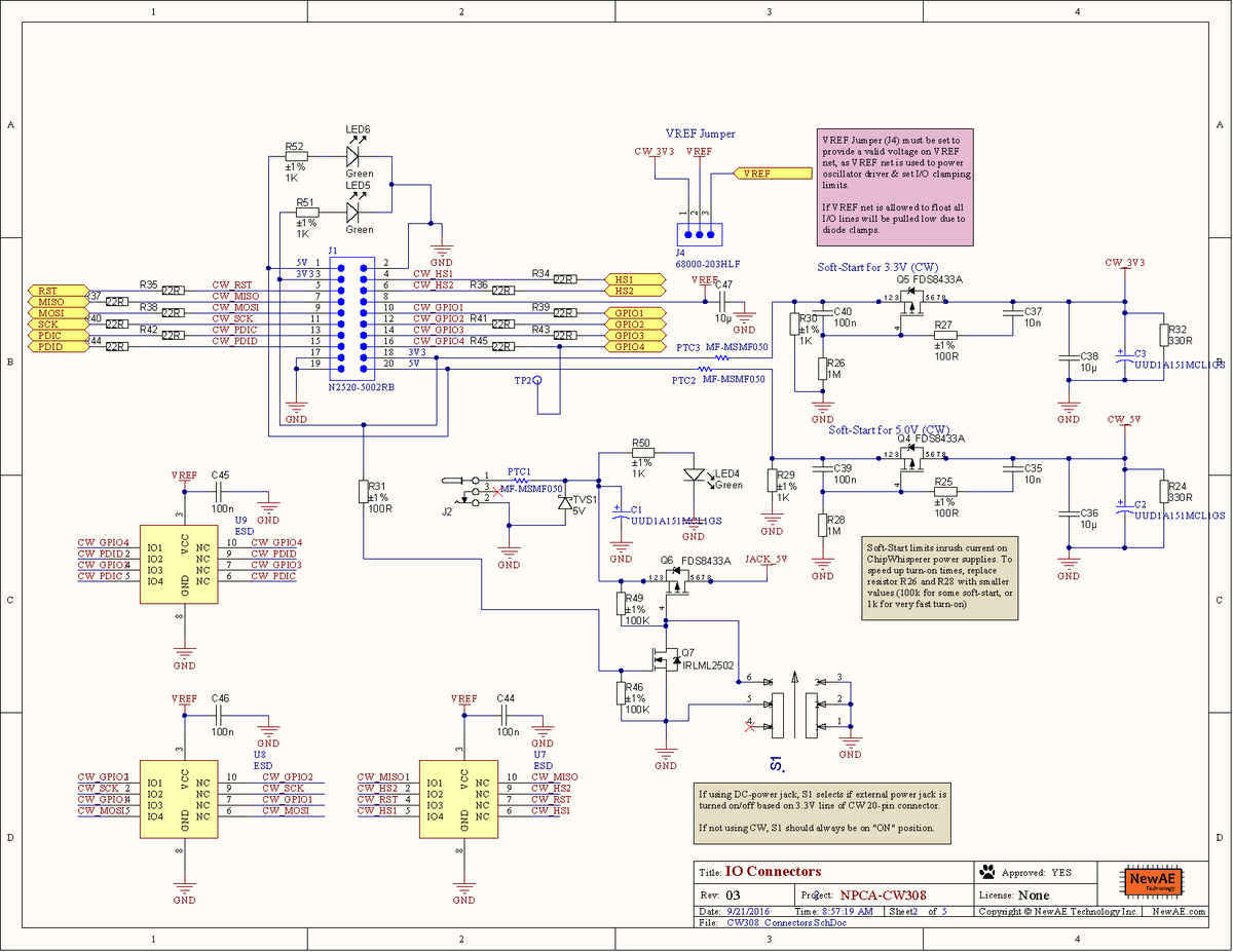
The ChipWhisperer header pins (most of the pins on header J5) have diode protection to set a maximum voltage level. The maximum voltage is set by the voltage present on the middle pin of J4.
VREF Level Setting
The on-board 'VREF' network sets the reference voltage to allow usage with multiple I/O levels. Note there are no voltage translators on-board, instead you can use the [CW506 Advanced Breakout Board] to provide voltage translation. One of the pins on the 20-pin connector outputs the reference voltage (VREF), so the CW506 knows what voltage level to translate I/O signals to.
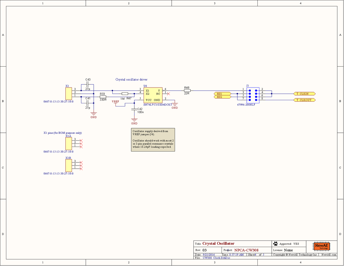
The on-board crystal oscillator is powered from the VREF network, ensuring the on-board oscillator is at an appropriate voltage reference.
The I/O pins connected to the 20-pin header have diode clamping, with the maximum level set by the VREF network. You must ensure jumper J4 sets a correct reference level. If using any of the official victim boards this is done by setting J4 to receive it's reference level from "J5-VREF" pin.
20-Pin Pinout
The pinout is as follows:
| Number | Name | Dir | Description |
|---|---|---|---|
| 1 | +5V | I | +5V from ChipWhisperer-Capture. |
| 2 | GND | I | System GND. |
| 3 | +3.3V | I | +3.3V from ChipWhisperer-Capture. |
| 4 | HS1 | O | High Speed output (normally clock in to ChipWhisperer-Capture). |
| 5 | nRST | I/O | Target RESET Pin (AVR Programmer). |
| 6 | HS2 | I | High Speed input (normally clock or glitch out from ChipWhisperer-Capture). |
| 7 | MISO | I/O | SPI input: MISO (for SPI + AVR Programmer). |
| 8 | VTarget | O | Set I/O voltage reference level. |
| 9 | MOSI | I/O | SPI output: MOSI (for SPI + AVR Programmer). |
| 10 | TARG1 | I/O | TargetIO Pin 1 - Usually UART TX or RX. |
| 11 | SCK | I/O | SPI output: SCK (for SPI + AVR Programmer). |
| 12 | GPIO2 | I/O | TargetIO Pin 2 - Usually UART RX or TX. |
| 13 | PROG-PDIC | I/O | PDI Programming Clock (XMEGA Programmer), or CS pin (SPI). |
| 14 | GPIO3 | I/O | TargetIO Pin 3 - Extra I/O. |
| 15 | PROG-PDID | I/O | PDI Programming Data (XMEGA Programmer). |
| 16 | GPIO4 | I/O | TargetIO Pin 4 - Usually trigger output. |
| 17 | GND | O | |
| 18 | +3.3V | O | +3.3V from ChipWhisperer-Capture. |
| 19 | GND | O | |
| 20 | +5V | O | +5V from ChipWhisperer-Capture. |
Clock Network
Crystal Driver
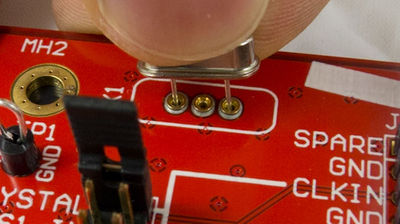
The CW308 contains a crystal oscillator driver. This allows you to use a standard crystal to drive either the victim board or the connected ChipWhisperer. This also allows the use of the CW308 stand-alone, as it's possible to generate almost any frequency by simply putting an appropriate crystal into the socket.
Clock Selection
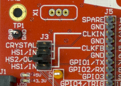
The clock routing is selected using jumper J3. This allows the following use cases:
- Routing crystal oscillator (X1) to victim CLKIN.
- Routing crystal oscillator (X1) to ChipWhisperer HS-IN, then routing HS-OUT to victim CLKIN (for glitch insertion).
- Routing CLKFB from victim to ChipWhisperer HS-IN.
- Routing ChipWhisperer HS-OUT to victim CLKIN.
Power Distribution
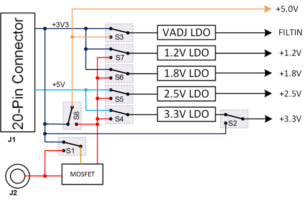
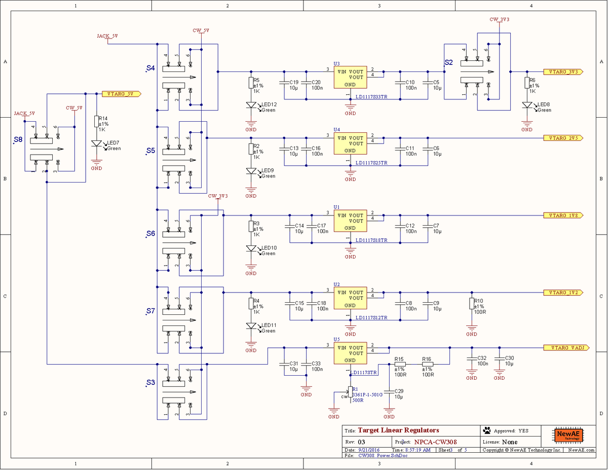
The following shows the routing of power to the victim board:
The following summarizes the switch information:
| Switch | Function | Location | Notes |
|---|---|---|---|
| S1 | Switch 5.0V from DC-Power Jack On/Off | Lower Left | Selects if DC 5.0V from DC-Jack is "always on", or gets gated by 3.3V source from 20-pin connector ('auto'). If 'auto' mode selected and no 20-pin cable connected, this is equivalent to turning the main supply to the board on/off. Thus when using the board stand-alone S1 acts as a power switch for the board. |
| S3 | Choose 5.0V source to connect to victim board. | Can be used to turn on/off 5.0V to victim board. | |
| S3-S7 | Selected fixed LDO input source. | Can be used to turn on/off certain LDOs. | |
| S8 | Select adjustable LDO input source. | Select 5.0V or 3.3V input (3.3V comes from ChipWhisperer). | |
| S2 | Choose 3.3V source to connect to victim board. | Select 3.3V from 20-pin ChipWhisperer cable, or local LDO. |
External Power Sources
There are two main sources to supply power to the CW308:
- DC-input power jack (2.1mm barrel jack, center positive, 5.0V)
- ChipWhisperer 20-pin connector (5.0V and 3.3V).
Note you can use the DC-input power jack alongside the ChipWhisperer power supply. The CW308 can switch the DC-power on/off, allowing the ChipWhisperer to still control the target power.
If using the board stand-alone, you can use the 3.3V pin of the CW20 pin to turn on/off the board remotely. This pin can be used as a digital input, which will turn on/off the 5.0V power jack. Be sure to switch all regulators to use the 5.0V DC-Jack in this case to avoid having a load on the 3.3V pin.
On-Board LDOs
There are five LDOs on-board the CW308. While they are mostly rated for 800mA, the board does not have sufficient thermal dissipation to operate at these conditions.
Four of the LDOs have fixed voltage settings: 1.2V, 1.8V, 2.5V, and 3.3V. The fifth LDO is adjustable, and is especially useful if you need to either (a) overcome the voltage drop of a shunt, or (b) feed a power supply into a device to turn off an internal regulator.
Adjustable Voltage Example
Power Filter
The CW308 contains a L-C low-pass filter. This filter is designed to provide a highly filtered version of the power supply to the victim board. The various voltages on the victim board power headers can be directly routed to the various required power pins. For example if your device has an on-board PLL, this power supply is something we do not need to measure as part of the power analysis.
The "core" voltage supply for the device should first be fed through the on-board filter. This is accomplished by feeding the desired voltage (for example a 1.8V supply) into the "FILT" pin (pin C8). The output of the filter will be present on the FILT_LP and FILT_HP pins. You can then feed this through your shunt resistor, and finally to the core voltage of the device being measured.
Note jumper J14 can be used to override the filter input voltage. This override can come from the adjustable regulator as previously mentioned.
Programmer Connections
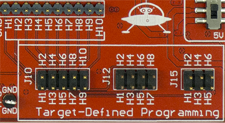
There are several headers that can be used as programming headers for the victim board. These are J10, J12, an J15. They are routed to pins 10 to 20 (H1 to H10) on the victim board connector J9. These connectors function is defined by the specific victim board mounted.
In addition there is a 20-pin JTAG header. This uses the standard JTAG ARM pinout.
Jumper Summary
J3: Clock selection.
Selects clock routing on the board. The following shows various examples of settings for this jumper:
| 1 | 2 | Meaning | |
|---|---|---|---|
| 1 | |||
| 2 | |||
| 3 | X | X | Sends clock from ChipWhisperer-Capture to Victim board. (DEFAULT) |
| 4 |
| 1 | 2 | Meaning | |
|---|---|---|---|
| 1 | X | X | Connect crystal oscillator output to CLKIN on Victim. |
| 2 | X | X | Also send clock to ChipWhisperer-Capture input for synchronization. |
| 3 | |||
| 4 |
| 1 | 2 | Meaning | |
|---|---|---|---|
| 1 | X | ||
| 2 | X | Route crystal oscillator to ChipWhisperer-Capture only (and not to target device). | |
| 3 | X | X | Route clock from ChipWhisperer-Capture to device (i.e., may be glitchy version of input clock). |
| 4 |
| 1 | 2 | Meaning | |
|---|---|---|---|
| 1 | |||
| 2 | |||
| 3 | |||
| 4 | X | X | Route clock from victim to ChipWhisperer-Capture for synchronization. |
J4: VREF selection.
Selects levels for the diode clamps, selects voltage set on ChipWhisperer 20-pin connector VREF pin, selects I/O level for crystal oscillator.
| 1 | 2 | 3 | Meaning |
|---|---|---|---|
| X | X | VREF Network set by VREF Pin from Victim Board (DEFAULT) | |
| X | X | VREF Network set to 3.3V from ChipWhisperer 20-pin header. If using board stand-alone this option cannot be used. | |
| VREF voltage can be fed into center pin via a jumper wire. |
J14: Filter input selection.
Selects source of FILT_IN pin. This pin can either come from the victim board (where victim sets own voltage), or the VADJ network (where adjustable regulator is used).
The adjustable regulator is often required when overcoming the voltage drop in the shunt and/or filter.
| 1 | 2 | 3 | Meaning |
|---|---|---|---|
| X | X | Filter input set by FILT Pin from Victim Board (DEFAULT) | |
| X | X | Filter input set by VADJ. Be sure to adjust voltage before using this. | |
| Filter voltage can be fed into center pin via a jumper wire. |
Usage Example: Stand-Alone
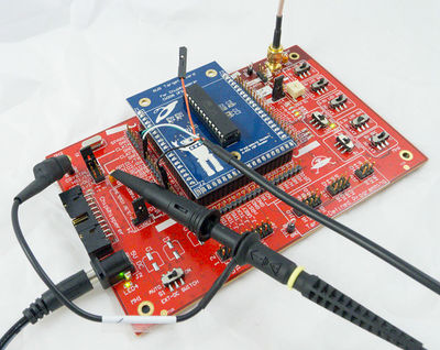
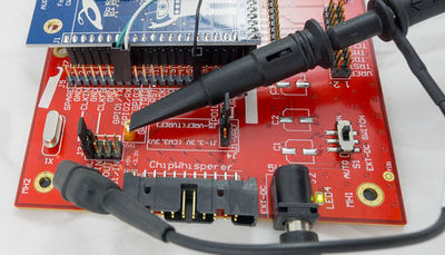
The CW308 can be used stand-alone. This is accomplished by providing an external DC power supply, and using a SMA-BNC to connect the voltage measurement to an oscilloscope. For more details, see CW308T: Stand-Alone Simple Serial Example (AVR or XMEGA).
If using a simple-serial target (such as the XMEGA or AVR), you can connect a USB-Serial device to provide communication.
Usage Hints
Schematic
The schematic is available in PDF format here: NAE-CW308-03 Schematic (PDF).
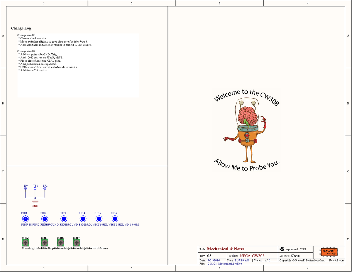
The following has a copy of schematic pages in image as well:
